ZHCSJE1C February 2019 – December 2023 TMUX1111 , TMUX1112 , TMUX1113
PRODUCTION DATA
- 1
- 1 特性
- 2 应用
- 3 说明
- 4 Device Comparison Table
- 5 Pin Configuration and Functions
-
6 Specifications
- 6.1 Absolute Maximum Ratings
- 6.2 ESD Ratings
- 6.3 Recommended Operating Conditions
- 6.4 Thermal Information
- 6.5 Electrical Characteristics (VDD = 5V ±10 %)
- 6.6 Electrical Characteristics (VDD = 3.3V ±10 %)
- 6.7 Electrical Characteristics (VDD = 1.8V ±10 %)
- 6.8 Electrical Characteristics (VDD = 1.2V ±10 %)
- 6.9 Typical Characteristics
- 7 Parameter Measurement Information
- 8 Detailed Description
- 9 Application and Implementation
- 10Device and Documentation Support
- 11Revision History
- 12Mechanical, Packaging, and Orderable Information
封装选项
请参考 PDF 数据表获取器件具体的封装图。
机械数据 (封装 | 引脚)
- PW|16
- RSV|16
散热焊盘机械数据 (封装 | 引脚)
订购信息
9.2 Typical Application - Sample-and-Hold Circuit
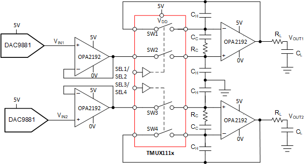
One useful application to take advantage of the TMUX1111, TMUX1112, and TMUX1113 performance is the sample-and-hold circuit. A sample-and-hold circuit can be useful for an analog to digital converter (ADC) to sample a varying input voltage with improved reliability and stability. It can also be used to store the output samples from a single digital-to-analog converter (DAC) in a multi-output application. A simple sample-and-hold circuit can be realized using an analog switch such as the TMUX1111, TMUX1112, and TMUX1113 analog switches. Figure 9-1 shows a single channel sample-and hold circuit using only 1 of 4 channels in the TMUX111x devices.
 Figure 9-1 Single Channel Sample-and-Hold Circuit Example
An optional op amp is used before the switch since buffered DACs typically have limitations in driving capacitive loads. The additional buffer stage is included following the DAC to prevent potential stability problems from driving a large capacitive load.
Ideally, the switch delivers only the input signals to the holding capacitors. However, when the switch gets toggled, some amount of charge also gets transferred to the switch output in the form of charge injection, resulting in a pedestal sampling error. The TMUX1111, TMUX1112, and TMUX1113 switches have excellent charge injection performance of only -1.5pC, making them excellent choices for this implementation to minimize sampling error. The pedestal error voltage is indirectly related to the size of the capacitance on the output, for better precision a larger capacitor is required due to charge injection. Larger capacitance limits the system settling time which may not be acceptable in some applications. Figure 9-2 shows a TMUX111x device configured for a 2-channel sample-and-hold circuit with pedestal error compensation.
 Figure 9-2 2-Channel Sample-and-Hold Circuit with Pedestal Error Compensation