ZHCSJM4A April 2019 – October 2019 TMUX1204
PRODUCTION DATA.
- 1 特性
- 2 应用
- 3 说明
- 4 修订历史记录
- 5 Pin Configuration and Functions
-
6 Specifications
- 6.1 Absolute Maximum Ratings
- 6.2 ESD Ratings
- 6.3 Recommended Operating Conditions
- 6.4 Thermal Information
- 6.5 Electrical Characteristics (VDD = 5 V ±10 %)
- 6.6 Electrical Characteristics (VDD = 3.3 V ±10 %)
- 6.7 Electrical Characteristics (VDD = 1.8 V ±10 %)
- 6.8 Electrical Characteristics (VDD = 1.2 V ±10 %)
- 6.9 Typical Characteristics
- 7 Parameter Measurement Information
- 8 Detailed Description
- 9 Application and Implementation
- 10Power Supply Recommendations
- 11Layout
- 12器件和文档支持
- 13机械、封装和可订购信息
封装选项
机械数据 (封装 | 引脚)
散热焊盘机械数据 (封装 | 引脚)
- DQA|10
订购信息
7.7 Charge Injection
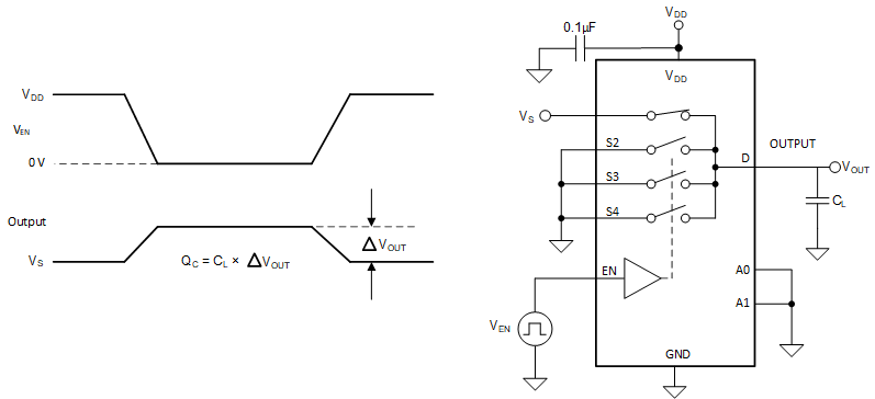
The TMUX1204 has a transmission-gate topology. Any mismatch in capacitance between the NMOS and PMOS transistors results in a charge injected into the drain or source during the falling or rising edge of the gate signal. The amount of charge injected into the source or drain of the device is known as charge injection, and is denoted by the symbol QC. Figure 13 shows the setup used to measure charge injection from source (Sx) to drain (D).
 Figure 13. Charge-Injection Measurement Setup