SCDS424A December 2019 – March 2020 TMUX1237
PRODUCTION DATA.
- 1 Features
- 2 Applications
- 3 Description
- 4 Revision History
- 5 Pin Configuration and Functions
-
6 Specifications
- 6.1 Absolute Maximum Ratings
- 6.2 ESD Ratings
- 6.3 Recommended Operating Conditions
- 6.4 Thermal Information
- 6.5 Electrical Characteristics (VDD = 5 V ±10 %), GND = 0 V unless otherwise specified.
- 6.6 Electrical Characteristics (VDD = 3.3 V ±10 %), GND = 0 V unless otherwise specified.
- 6.7 Electrical Characteristics (VDD = 1.8 V ±10 %), GND = 0 V unless otherwise specified.
- 6.8 Electrical Characteristics (VDD = 1.2 V ±10 %), GND = 0 V unless otherwise specified.
- 6.9 Typical Characteristics
- 7 Parameter Measurement Information
- 8 Detailed Description
- 9 Application and Implementation
- 10Power Supply Recommendations
- 11Layout
- 12Device and Documentation Support
- 13Mechanical, Packaging, and Orderable Information
9.2.1 Input Control for Power Amplifier
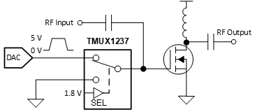
One application of the TMUX1237 is for input control of a power amplifier. Utilizing a switch allows a system to control when the DAC is connected to the power amplifier, and can stop biasing the power amplifier by switching the gate to GND. Figure 17 shows the TMUX1237 configured for control of the power amplifier. The no overshoot when switching between inputs feature of the TMUX1237 is beneficial in applications such as this where the output is being switched across the full voltage range, and any overshoot on the output is undesired.
 Figure 17. Input Control of Power Amplifier