ZHCSLR4F december   2019  – july 2023 TMUX1308-Q1 , TMUX1309-Q1

PRODUCTION DATA  

  1.   1
  2. 特性
  3. 应用
  4. 说明
  5. Revision History
  6. Device Comparison Table
  7. Pin Configuration and Functions
  8. Specifications
    1. 7.1  Absolute Maximum Ratings
    2. 7.2  ESD Ratings
    3. 7.3  Recommended Operating Conditions
    4. 7.4  Thermal Information: TMUX1308-Q1
    5. 7.5  Thermal Information: TMUX1309-Q1
    6. 7.6  Electrical Characteristics
    7. 7.7  Logic and Dynamic Characteristics
    8. 7.8  Timing Characteristics
    9. 7.9  Injection Current Coupling
    10. 7.10 Typical Characteristics
  9. Parameter Measurement Information
    1. 8.1  On-Resistance
    2. 8.2  Off-Leakage Current
    3. 8.3  On-Leakage Current
    4. 8.4  Transition Time
    5. 8.5  Break-Before-Make
    6. 8.6  tON(EN) and tOFF(EN)
    7. 8.7  Charge Injection
    8. 8.8  Off Isolation
    9. 8.9  Crosstalk
    10. 8.10 Bandwidth
    11. 8.11 Injection Current Control
  10. Detailed Description
    1. 9.1 Overview
    2. 9.2 Functional Block Diagram
    3. 9.3 Feature Description
      1. 9.3.1 Bidirectional Operation
      2. 9.3.2 Rail-to-Rail Operation
      3. 9.3.3 1.8 V Logic Compatible Inputs
      4. 9.3.4 Fail-Safe Logic
      5. 9.3.5 Injection Current Control
        1. 9.3.5.1 TMUX13xx-Q1 is Powered, Channel is Unselected, and the Input Signal is Greater Than VDD (VDD = 5 V, VINPUT = 5.5 V)
        2. 9.3.5.2 TMUX13xx-Q1 is Powered, Channel is Selected, and the Input Signal is Greater Than VDD (VDD = 5 V, VINPUT = 5.5 V)
        3. 9.3.5.3 TMUX13xx-Q1 is Unpowered and the Input Signal has a Voltage Present (VDD = 0 V, VINPUT = 3 V)
    4. 9.4 Device Functional Modes
    5. 9.5 Truth Tables
  11. 10Application and Implementation
    1. 10.1 Application Information
    2. 10.2 Typical Application
      1. 10.2.1 Design Requirements
      2. 10.2.2 Detailed Design Procedure
      3. 10.2.3 Short To Battery Protection
    3. 10.3 Power Supply Recommendations
    4. 10.4 Layout
      1. 10.4.1 Layout Guidelines
      2. 10.4.2 Layout Example
  12. 11Device and Documentation Support
    1. 11.1 Documentation Support
      1. 11.1.1 Related Documentation
    2. 11.2 Receiving Notification of Documentation Updates
    3. 11.3 支持资源
    4. 11.4 Trademarks
    5. 11.5 静电放电警告
    6. 11.6 术语表
  13. 12Mechanical, Packaging, and Orderable Information

封装选项

机械数据 (封装 | 引脚)
散热焊盘机械数据 (封装 | 引脚)
订购信息

Typical Characteristics

at TA = 25°C, VDD = 5 V (unless otherwise noted)
GUID-76B9D7B4-6BC8-4D87-8FB7-B5F750AA6090-low.gif
VDD = 5 V
Figure 7-1 On-Resistance vs Temperature
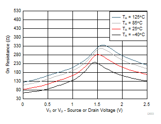
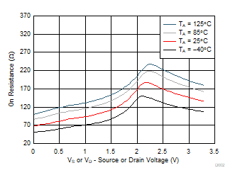
GUID-2A768B51-C78E-4C6E-8FB3-7CD75091A514-low.gif
VDD = 2.5 V
Figure 7-3 On-Resistance vs Temperature
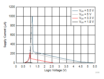
GUID-0BC748A5-09DC-4308-9725-F76877492E74-low.gif
Figure 7-5 Supply Current vs Logic Voltage
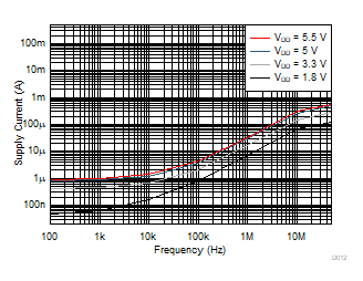
GUID-2E8774FC-D13D-43AE-ABE5-1DD0281FF100-low.gif
TA = 25°C
Figure 7-7 Supply Current vs Input Switching Frequency
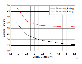
GUID-1637AC81-D2E0-4670-AD37-721AEE8092D6-low.gif
TA = 25°C
Figure 7-9 TTRANSITION vs Supply Voltage
GUID-B3CFDE2A-2454-40BA-8317-7A1CDCBBF619-low.gif
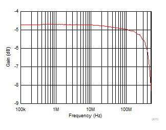
TA = 25°C
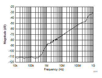
Figure 7-11 On Response vs Frequency
GUID-D092B430-D9F3-4238-BB5A-33818BD0EE8D-low.gif
VS = (VDD/2), TA = 25°C
Figure 7-13 Injection Current vs Maximum Output Voltage Shift
GUID-80D7CEE4-27A4-47A5-A093-711550012440-low.gif
VDD = 3.3 V
Figure 7-2 On-Resistance vs Temperature
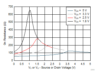
GUID-A18EDC84-8E63-44A4-AF18-F0BD246BAFA5-low.gif
TA = 25°C
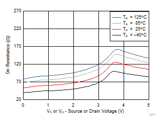
Figure 7-4 On-Resistance vs Source or Drain Voltage
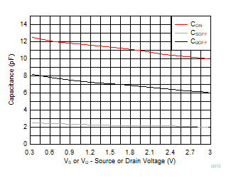
GUID-55AB6547-B69E-4D79-B11D-289FA1976335-low.gif
VDD = 3.3 V
Figure 7-6 Capacitance vs Source Voltage
GUID-CC2C50AE-A4F9-4AB4-BEE6-33517CE45D41-low.gif
VDD = 3.3 V
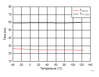
Figure 7-8 TON(EN) and TOFF(EN) vs Temperature
GUID-5565896C-EC93-452B-8E51-061AEA001098-low.gif
TA = 25°C
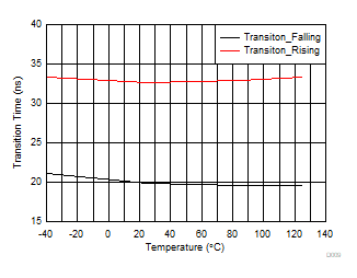
Figure 7-10 TTRANSITION vs Temperature
GUID-EF90CA2E-9550-4453-A723-AA6A9A1F6AF7-low.gif
TA = 25°C , VDD = 3.3 V
Figure 7-12 Xtalk and Off-Isolation vs Frequency