ZHCSLR4F december 2019 – july 2023 TMUX1308-Q1 , TMUX1309-Q1
PRODUCTION DATA
- 1
- 1 特性
- 2 应用
- 3 说明
- 4 Revision History
- 5 Device Comparison Table
- 6 Pin Configuration and Functions
-
7 Specifications
- 7.1 Absolute Maximum Ratings
- 7.2 ESD Ratings
- 7.3 Recommended Operating Conditions
- 7.4 Thermal Information: TMUX1308-Q1
- 7.5 Thermal Information: TMUX1309-Q1
- 7.6 Electrical Characteristics
- 7.7 Logic and Dynamic Characteristics
- 7.8 Timing Characteristics
- 7.9 Injection Current Coupling
- 7.10 Typical Characteristics
- 8 Parameter Measurement Information
-
9 Detailed Description
- 9.1 Overview
- 9.2 Functional Block Diagram
- 9.3
Feature Description
- 9.3.1 Bidirectional Operation
- 9.3.2 Rail-to-Rail Operation
- 9.3.3 1.8 V Logic Compatible Inputs
- 9.3.4 Fail-Safe Logic
- 9.3.5
Injection Current Control
- 9.3.5.1 TMUX13xx-Q1 is Powered, Channel is Unselected, and the Input Signal is Greater Than VDD (VDD = 5 V, VINPUT = 5.5 V)
- 9.3.5.2 TMUX13xx-Q1 is Powered, Channel is Selected, and the Input Signal is Greater Than VDD (VDD = 5 V, VINPUT = 5.5 V)
- 9.3.5.3 TMUX13xx-Q1 is Unpowered and the Input Signal has a Voltage Present (VDD = 0 V, VINPUT = 3 V)
- 9.4 Device Functional Modes
- 9.5 Truth Tables
- 10Application and Implementation
- 11Device and Documentation Support
- 12Mechanical, Packaging, and Orderable Information
封装选项
机械数据 (封装 | 引脚)
散热焊盘机械数据 (封装 | 引脚)
- BQB|16
订购信息
10.2.2 Detailed Design Procedure
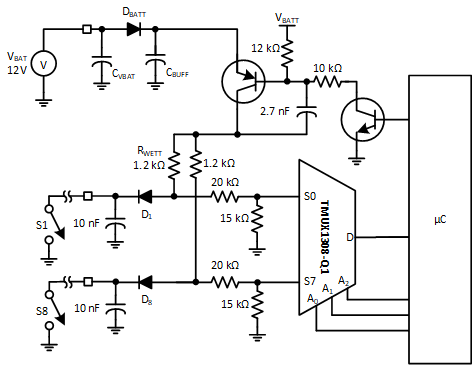
The TMUX1308-Q1 has an internal injection current control feature which eliminates the need for external diode or resistor networks typically used to protect the switch and keep the input signals within the supply voltage. The internal injection current control circuitry allows signals on disabled signal paths to exceed the supply voltage without affecting the signal of the enabled signal path. Injected currents can come from various sources such as from long cabling in automotive systems that may be susceptible to induced currents from switching or transient events. Another momentary source of injected currents in BCMs are wetting currents, which are small currents used to prevent oxidation on metal switch contacts or wires. A switch without injection current control can have the measured output of the enabled signal path impacted if a current is injected into a disabled signal path. This undesired change in the output can cause issues related to false trigger events and incorrect measurement readings which can compromise the accuracy and reliability of the BCM system. Figure 10-2 shows a detailed BCM application.
 Figure 10-2 Detailed BCM Application
The BCM uses the 12 V battery voltage to provide a wetting current to each switch when the associated control circuitry is enabled by the micro controller. The wetting current is sized by the RWETT and the required value may vary depending on the type of physical switch being monitored. The 20 kΩ and 15 kΩ resistors are used in addition to the wetting resistor to create a voltage divider before the input of the multiplexer in case of a short to battery condition. The resistor values are selected to maintain the voltage at the switch signal path below VDD. The 20 kΩ series resistor also limits the amount of injected current into the switch if an overvoltage event occurs. Diodes D1 through D8 are used to prevent back flow of current in case a secondary system is monitoring the same physical switches for backup or redundancy reasons. The 10 nF capacitors are used for initial ESD protection in the system and must be sized based on system level requirements.
The logic address pins are controlled by the micro controller to cycle between the eight switch inputs in the system. If the parts desired power-up state is disabled, then the enable pin should have a weak pull-up resistor and be controlled by the MCU through the GPIO.