ZHCSIR9A September   2018  – December 2018 TMUX1511

PRODUCTION DATA.  

  1. 特性
  2. 应用
  3. 说明
    1.     Device Images
      1.      应用示例
      2.      方框图
  4. 修订历史记录
  5. Pin Configuration and Functions
    1.     Pin Functions
  6. Specifications
    1. 6.1 Absolute Maximum Ratings
    2. 6.2 ESD Ratings
    3. 6.3 Recommended Operating Conditions
    4. 6.4 Thermal Information
    5. 6.5 Electrical Characteristics
    6. 6.6 Dynamic Characteristics
    7. 6.7 Timing Requirements
    8. 6.8 Typical Characteristics
      1. 6.8.1 Eye Diagrams
  7. Parameter Measurement Information
    1. 7.1  On-Resistance
    2. 7.2  Off-Leakage Current
    3. 7.3  On-Leakage Current
    4. 7.4  IPOFF Leakage Current
    5. 7.5  Transition Time
    6. 7.6  TON (VDD) and TOFF (VDD) Time
    7. 7.7  Propagation Delay
    8. 7.8  Skew
    9. 7.9  Charge Injection
    10. 7.10 Capacitance
    11. 7.11 Off Isolation
    12. 7.12 Channel-to-Channel Crosstalk
    13. 7.13 Bandwidth
  8. Detailed Description
    1. 8.1 Overview
    2. 8.2 Functional Block Diagram
    3. 8.3 Feature Description
      1. 8.3.1 Bidirectional Operation
      2. 8.3.2 Beyond Supply Operation
      3. 8.3.3 1.8 V Logic Compatible Inputs
      4. 8.3.4 Powered-off Protection
      5. 8.3.5 Fail-Safe Logic
      6. 8.3.6 Low Capacitance
      7. 8.3.7 Integrated Pull-Down Resistors
    4. 8.4 Device Functional Modes
    5. 8.5 Truth Tables
  9. Application and Implementation
    1. 9.1 Application Information
    2. 9.2 Typical Application
      1. 9.2.1 Protocol / Signal Isolation
        1. 9.2.1.1 Design Requirements
        2. 9.2.1.2 Detailed Design Procedure
        3. 9.2.1.3 Application Curves
      2. 9.2.2 Transimpedance Amplifier Feedback Control
        1. 9.2.2.1 Design Requirements
        2. 9.2.2.2 Detailed Design Procedure
        3. 9.2.2.3 Application Curves
  10. 10Power Supply Recommendations
  11. 11Layout
    1. 11.1 Layout Guidelines
    2. 11.2 Layout Example
  12. 12器件和文档支持
    1. 12.1 文档支持
      1. 12.1.1 相关文档
    2. 12.2 接收文档更新通知
    3. 12.3 社区资源
    4. 12.4 商标
    5. 12.5 静电放电警告
    6. 12.6 术语表
  13. 13机械、封装和可订购信息

封装选项

机械数据 (封装 | 引脚)
散热焊盘机械数据 (封装 | 引脚)
订购信息

On-Resistance

The on-resistance of a device is the ohmic resistance between the source (Sx) and drain (Dx) pins of the device. The on-resistance varies with input voltage and supply voltage. The symbol RON is used to denote on-resistance. The measurement setup used to measure RON is shown in Figure 27 . Voltage (V) and current (IDS) are measured using this setup, and RON is computed as shown below with RON = V / ISD:
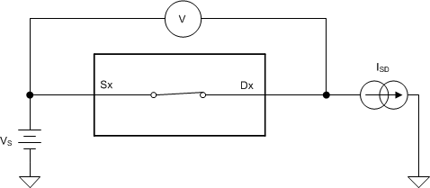
TMUX1511 On_Resistance.gifFigure 27. On-Resistance Measurement Setup