ZHCSIN7E August 2018 – December 2019 TMUX6111 , TMUX6112 , TMUX6113
PRODUCTION DATA.
- 1 特性
- 2 应用
- 3 说明
- 4 修订历史记录
- 5 Device Comparison Table
- 6 Pin Configuration and Functions
-
7 Specifications
- 7.1 Absolute Maximum Ratings
- 7.2 ESD Ratings
- 7.3 Thermal Information
- 7.4 Recommended Operating Conditions
- 7.5 Electrical Characteristics (Dual Supplies: ±15 V)
- 7.6 Switching Characteristics (Dual Supplies: ±15 V)
- 7.7 Electrical Characteristics (Single Supply: 12 V)
- 7.8 Switching Characteristics (Single Supply: 12 V)
- 7.9 Typical Characteristics
- 8 Parameter Measurement Information
- 9 Detailed Description
- 10Application and Implementation
- 11Power Supply Recommendations
- 12Layout
- 13器件和文档支持
- 14机械、封装和可订购信息
封装选项
机械数据 (封装 | 引脚)
散热焊盘机械数据 (封装 | 引脚)
- RTE|16
订购信息
9.3.2 Ultra-low Charge Injection
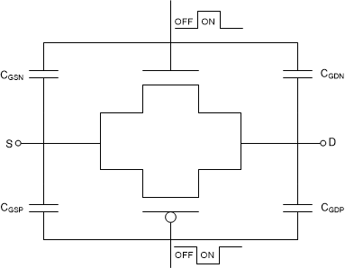
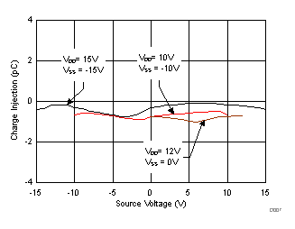
The TMUX6111, TMUX6112, and TMUX6113 are implemented with simple transmission gate topology, as shown in Figure 28. Any mismatch in the stray capacitance associated with the NMOS and PMOS causes an output level change whenever the switch is opened or closed. The devices utilize special charge-injection cancellation circuitry that reduces the source (Sx)-to-drain (Dx) charge injection to as low as 0.6 pC at VS = 0 V, as shown in Figure 29.
 Figure 28. Transmission Gate Topology
  Figure 29. Source-to-Drain Charge Injection vs Source or Drain Voltage