ZHCSIN7E August 2018 – December 2019 TMUX6111 , TMUX6112 , TMUX6113
PRODUCTION DATA.
- 1 特性
- 2 应用
- 3 说明
- 4 修订历史记录
- 5 Device Comparison Table
- 6 Pin Configuration and Functions
-
7 Specifications
- 7.1 Absolute Maximum Ratings
- 7.2 ESD Ratings
- 7.3 Thermal Information
- 7.4 Recommended Operating Conditions
- 7.5 Electrical Characteristics (Dual Supplies: ±15 V)
- 7.6 Switching Characteristics (Dual Supplies: ±15 V)
- 7.7 Electrical Characteristics (Single Supply: 12 V)
- 7.8 Switching Characteristics (Single Supply: 12 V)
- 7.9 Typical Characteristics
- 8 Parameter Measurement Information
- 9 Detailed Description
- 10Application and Implementation
- 11Power Supply Recommendations
- 12Layout
- 13器件和文档支持
- 14机械、封装和可订购信息
封装选项
机械数据 (封装 | 引脚)
散热焊盘机械数据 (封装 | 引脚)
- RTE|16
订购信息
10.2 Typical Application
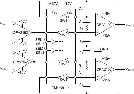
One useful application to take advantage of TMUX6111, TMUX6112, and TMUX6113's precision performance is the sample and hold circuit. A sample and hold circuit can be useful for an analog to digital converter (ADC) to sample a varying input voltage with improved reliability and stability. It can also be used to store the output samples from a single digital-to-analog converter (DAC) in a multi-output application. A simple sample and hold circuit can be realized using an analog switch like one of the TMUX6111, TMUX6112, and TMUX6113 analog switches.
