ZHCSJ28A November 2018 – October 2022 TMUX6136
PRODUCTION DATA
- 1 特性
- 2 应用
- 3 说明
- 4 Revision History
- 5 Pin Configuration and Functions
-
6 Specifications
- 6.1 Absolute Maximum Ratings
- 6.2 ESD Ratings
- 6.3 Thermal Information
- 6.4 Recommended Operating Conditions
- 6.5 Electrical Characteristics (Dual Supplies: ±15 V)
- 6.6 Switching Characteristics (Dual Supplies: ±15 V)
- 6.7 Electrical Characteristics (Single Supply: 12 V)
- 6.8 Switching Characteristics (Single Supply: 12 V)
- Typical Characteristics
- 7 Detailed Description
- 8 Application and Implementation
- 9 Power Supply Recommendations
- 10Layout
- 11Device and Documentation Support
- 12Mechanical, Packaging, and Orderable Information
8.2.2 Detailed Design Procedure
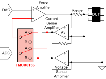
 Figure 8-3 FVMC Implementation in PMU
Using the TMUX6136
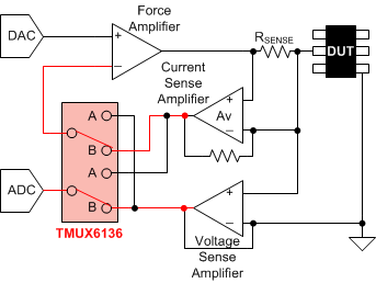
 Figure 8-4 FCMV Implementation in PMU
Using the TMUX6136
Figure 8-4 FCMV Implementation in PMU
Using the TMUX6136The implementation of the FVMC and FCMV modes can be combined with the use of a dual SPDT switch such as the TMUX6136. Figure 8-3 and Figure 8-4 shows simplified diagrams of such implementations. In the FVMC mode, the switch is toggled to position A and this allows the voltage sense amplifier to become part of the feedback loop and the voltage output of the current sense amplifier to be sampled by the ADC. In the FCMV mode, the switch is toggled to position B, and this allows the current sense amplifier to become part of the feedback loop and the voltage output of the voltage sense amplifier to be sampled by the ADC.