ZHCSNM9B march 2021 – june 2023 TMUX7462F
PRODUCTION DATA
- 1
- 1 特性
- 2 应用
- 3 说明
- 4 Revision History
- 5 Pin Configuration and Functions
-
6 Specifications
- 6.1 Absolute Maximum Ratings
- 6.2 ESD Ratings
- 6.3 Thermal Information
- 6.4 Recommended Operating Conditions
- 6.5 Electrical Characteristics (Global)
- 6.6 ±15 V Dual Supply: Electrical Characteristics
- 6.7 ±20 V Dual Supply: Electrical Characteristics
- 6.8 12 V Single Supply: Electrical Characteristics
- 6.9 36 V Single Supply: Electrical Characteristics
- 6.10 Typical Characteristics
- 7 Parameter Measurement Information
- 8 Detailed Description
- 9 Application and Implementation
- 10Device and Documentation Support
- 11Mechanical, Packaging, and Orderable Information
5 Pin Configuration and Functions
 Figure 5-1 PW Package, 16-Pin TSSOP (Top View)
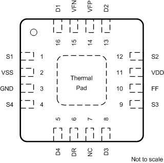
 Figure 5-2 RRP Package, 16-Pin WQFN (Top View)
Table 5-1 Pin Functions
| PIN | TYPE(1) | DESCRIPTION | ||
|---|---|---|---|---|
| NAME | TSSOP | WQFN | ||
| D1 | 2 | 16 | I/O | Drain pin 1 can be an input or output. The drain pin is not overvoltage protected and shall remain within the recommended operating range. |
| D2 | 15 | 13 | I/O | Drain pin 2 can be an input or output. The drain pin is not overvoltage protected and shall remain within the recommended operating range. |
| D3 | 10 | 8 | I/O | Drain pin 3 can be an input or output. The drain pin is not overvoltage protected and shall remain within the recommended operating range. |
| D4 | 7 | 5 | I/O | Drain pin 4 can be an input or output. The drain pin is not overvoltage protected and shall remain within the recommended operating range. |
| DR | 8 | 6 | I | Drain Response (DR) input. Tying the DR pin to GND enables the drain to be pulled to VFP or VFN through a 40 kΩ resistor during an overvoltage fault event. The drain pin becomes open circuit when the DR pin is a logic high or left floating. |
| FF | 12 | 10 | O | General fault flag. This pin is an open drain output and is asserted low when overvoltage condition is detected on any of the source (Sx) pins. Connect this pin to an external supply (1.8 V to 5.5 V) through a 1 kΩ pull-up resistor. |
| GND | 5 | 3 | P | Ground (0 V) reference. |
| N.C. | 9 | 7 | — | No internal connection |
| S1 | 3 | 1 | I/O | Overvoltage protected source pin 1 can be an input or output. |
| S2 | 14 | 12 | I/O | Overvoltage protected source pin 2 can be an input or output. |
| S3 | 11 | 9 | I/O | Overvoltage protected source pin 3 can be an input or output. |
| S4 | 6 | 4 | I/O | Overvoltage protected source pin 4 can be an input or output. |
| VDD | 13 | 11 | P | Positive power supply. This pin is the most positive power-supply potential. Connect a decoupling capacitor ranging from 0.1 µF to 10 µF between VDD and GND for reliable operation. |
| VFP | 16 | 14 | P | Positive fault voltage supply that determines the overvoltage protection triggering threshold on the positive side. Connect to VDD if the triggering threshold is the same as the device's positive supply. Connect a decoupling capacitor ranging from 0.1 µF to 10 µF between VFP and GND for reliable operation. |
| VFN | 1 | 15 | P | Negative fault voltage supply that determines the overvoltage protection triggering threshold on the negative side. Connect to VSS if the triggering threshold is the same as the device's negative supply. Connect a decoupling capacitor ranging from 0.1 µF to 10 µF between VFN and GND for reliable operation. |
| VSS | 4 | 2 | P | Negative power supply. This pin is the most negative power-supply potential. This pin can be connected to ground in single-supply applications. Connect a decoupling capacitor ranging from 0.1 µF to 10 µF between VSS and GND for reliable operation. |
| Thermal Pad | — | The thermal pad is not connected internally. No requirement to solder this pad. For best performance it is recommended that the pad be tied to GND or VSS. | ||
(1) I = input, O = output, I/O = input and output, P = power.