ZHCSNM9B march   2021  – june 2023 TMUX7462F

PRODUCTION DATA  

  1.   1
  2. 特性
  3. 应用
  4. 说明
  5. Revision History
  6. Pin Configuration and Functions
  7. Specifications
    1. 6.1  Absolute Maximum Ratings
    2. 6.2  ESD Ratings
    3. 6.3  Thermal Information
    4. 6.4  Recommended Operating Conditions
    5. 6.5  Electrical Characteristics (Global)
    6. 6.6  ±15 V Dual Supply: Electrical Characteristics
    7. 6.7  ±20 V Dual Supply: Electrical Characteristics
    8. 6.8  12 V Single Supply: Electrical Characteristics
    9. 6.9  36 V Single Supply: Electrical Characteristics
    10. 6.10 Typical Characteristics
  8. Parameter Measurement Information
    1. 7.1  On-Resistance
    2. 7.2  On-Leakage Current
    3. 7.3  Input and Output Leakage Current under Overvoltage Fault
    4. 7.4  Fault Response Time
    5. 7.5  Fault Recovery Time
    6. 7.6  Fault Flag Response Time
    7. 7.7  Fault Flag Recovery Time
    8. 7.8  Fault Drain Enable Time
    9. 7.9  Inter-Channel Crosstalk
    10. 7.10 Bandwidth
    11. 7.11 THD + Noise
  9. Detailed Description
    1. 8.1 Overview
    2. 8.2 Functional Block Diagram
    3. 8.3 Feature Description
      1. 8.3.1 Flat ON-Resistance
      2. 8.3.2 Protection Features
        1. 8.3.2.1 Input Voltage Tolerance
        2. 8.3.2.2 Powered-Off Protection
        3. 8.3.2.3 Fail-Safe Logic
        4. 8.3.2.4 Overvoltage Protection and Detection
        5. 8.3.2.5 Latch-Up Immunity
        6. 8.3.2.6 EMC Protection
      3. 8.3.3 Overvoltage Fault Flags
      4. 8.3.4 Bidirectional Operation
    4. 8.4 Device Functional Modes
      1. 8.4.1 Normal Mode
      2. 8.4.2 Fault Mode
      3. 8.4.3 Truth Table
  10. Application and Implementation
    1. 9.1 Application Information
    2. 9.2 Typical Application
      1. 9.2.1 Design Requirements
      2. 9.2.2 Detailed Design Procedure
      3. 9.2.3 Application Curves
    3. 9.3 Power Supply Recommendations
    4. 9.4 Layout
      1. 9.4.1 Layout Guidelines
      2. 9.4.2 Layout Example
  11. 10Device and Documentation Support
    1. 10.1 Documentation Support
      1. 10.1.1 Related Documentation
    2. 10.2 接收文档更新通知
    3. 10.3 支持资源
    4. 10.4 Trademarks
    5. 10.5 静电放电警告
    6. 10.6 术语表
  12. 11Mechanical, Packaging, and Orderable Information

封装选项

机械数据 (封装 | 引脚)
散热焊盘机械数据 (封装 | 引脚)
订购信息

Fault Drain Enable Time

tRESPONSE(DR) represents the delay between the voltage at the DR pin falling from a high to low signal and the output of the drain pin reaching 90% of the fault supplies (VFP or VFN). tRESPONSE(DR) is a measure of how quickly the internal pull-up engages in response to the DR pin. Figure 7-9 shows the setup used to measure tRESPONSE(DR).
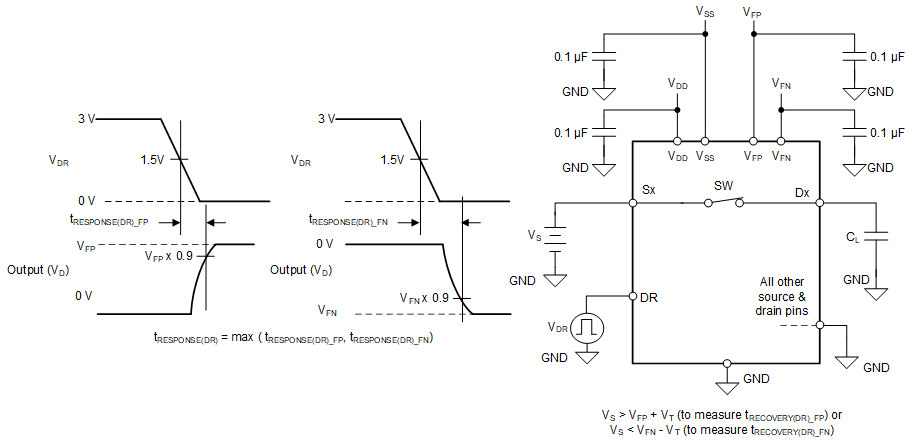
GUID-20211018-SS0I-SR3Z-LBJG-39PLHG9F8F47-low.gifFigure 7-9 Fault Drain Enable Time Measurement Setup