ZHCSNM9B march 2021 – june 2023 TMUX7462F
PRODUCTION DATA
- 1
- 1 特性
- 2 应用
- 3 说明
- 4 Revision History
- 5 Pin Configuration and Functions
-
6 Specifications
- 6.1 Absolute Maximum Ratings
- 6.2 ESD Ratings
- 6.3 Thermal Information
- 6.4 Recommended Operating Conditions
- 6.5 Electrical Characteristics (Global)
- 6.6 ±15 V Dual Supply: Electrical Characteristics
- 6.7 ±20 V Dual Supply: Electrical Characteristics
- 6.8 12 V Single Supply: Electrical Characteristics
- 6.9 36 V Single Supply: Electrical Characteristics
- 6.10 Typical Characteristics
- 7 Parameter Measurement Information
- 8 Detailed Description
- 9 Application and Implementation
- 10Device and Documentation Support
- 11Mechanical, Packaging, and Orderable Information
8.3.2.4 Overvoltage Protection and Detection
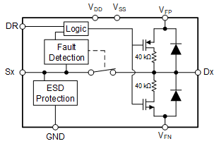
The TMUX7462F detects overvoltage inputs by comparing the voltage on a source pin (Sx) with the fault supplies (VFP and VFN). A signal is considered overvoltage if it exceeds the fault supply voltages by the threshold voltage (VT).
The switch automatically turns OFF and the source pin becomes high impedance so that only small leakage currents flow through the switch when an overvoltage is detected. The drain pin (Dx) behavior can be adjusted by controlling the drain response (DR) pin in the following ways:
- DR pin floating or driven above VIH:
If the DR pin is driven about VIH level of the pin, then the drain pin becomes high impedance (Hi-Z) upon overvoltage fault.
- DR driven below VIL:
If the DR pin is driven below VIL level of the pin, then the drain pin (Dx) is pulled to the supply that was exceeded. For example, if the source voltage exceeds VFP, then the drain output is pulled to VFP. If the source voltage exceeds VFN, then the drain output is pulled to VFN. The pull-up impedance is approximately 40 kΩ, and as a result, the drain current is limited to roughly 1 mA during a shorted load (to GND) condition.
Figure 9-3 shows a detailed view of the how the DR pin controls the output state of the drain pin under a fault scenario.
 Figure 8-1 Detailed Functional
Diagram
Figure 8-1 Detailed Functional
DiagramVFP and VFN are required fault supplies that set the level at which the overvoltage protection is engaged. VFP can be supplied from 3 V to VDD, while the VFN can be supplied from VSS to 0 V. If the fault supplies are not available in the system, then the VFP pin must be connected to VDD, while the VFN pin must be connected to VSS. In this case, the overvoltage protection then engages at the primary supply voltages VDD and VSS.