ZHCSM60B september 2021 – august 2023 TMUX8108 , TMUX8109
PRODUCTION DATA
- 1
- 1 特性
- 2 应用
- 3 说明
- 4 Revision History
- 5 Device Comparison Table
- 6 Pin Configuration and Functions
-
7 Specifications
- 7.1 Absolute Maximum Ratings: TMUX810x Devices
- 7.2 ESD Ratings
- 7.3 Recommended Operating Conditions: TMUX810x Devices
- 7.4 Thermal Information
- 7.5 Electrical Characteristics (Global): TMUX810x Devices
- 7.6 Electrical Characteristics (±15-V Dual Supply)
- 7.7 Electrical Characteristics (±36-V Dual Supply)
- 7.8 Electrical Characteristics (±50-V Dual Supply)
- 7.9 Electrical Characteristics (72-V Single Supply)
- 7.10 Electrical Characteristics (100-V Single Supply)
- 7.11 Switching Characteristics: TMUX810x Devices
- 7.12 Typical Characteristics
- 8 Parameter Measurement Information
- 9 Detailed Description
- 10Application and Implementation
- 11Device and Documentation Support
- 12Mechanical, Packaging, and Orderable Information
封装选项
请参考 PDF 数据表获取器件具体的封装图。
机械数据 (封装 | 引脚)
- PW|16
- RUM|16
散热焊盘机械数据 (封装 | 引脚)
- RUM|16
订购信息
8.3 On-Leakage Current
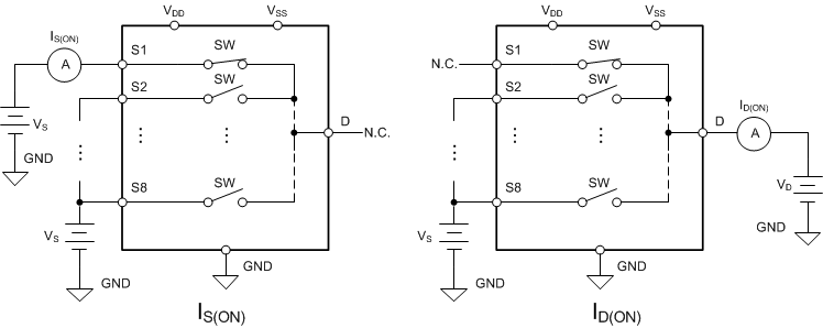
Source on-leakage current (IS(ON)) and drain on-leakage current (ID(ON)) denote the channel leakage currents when the switch is in the on state. IS(ON) is measured with the drain floating, while ID(ON) is measured with the source floating. Figure 8-3 shows the circuit used for measuring the on-leakage currents.
 Figure 8-3 On-Leakage Measurement Setup