ZHCSSN8 july   2023 TMUXHS221LV

PRODUCTION DATA  

  1.   1
  2. 特性
  3. 应用
  4. 说明
  5. Revision History
  6. Pin Configuration and Functions
  7. Specifications
    1. 6.1  Absolute Maximum Ratings
    2. 6.2  ESD Ratings
    3. 6.3  Recommended Operating Conditions
    4. 6.4  Thermal Information
    5. 6.5  Electrical Characteristics
    6. 6.6  High-Speed Performance Parameters
    7. 6.7  Switching Characteristics
    8. 6.8  Typical Characteristics – S-Parameters
    9. 6.9  Typical Characteristics – RON
    10. 6.10 Typical Characteristics – Eye Diagrams
    11.     18
  8. Detailed Description
    1. 7.1 Overview
    2. 7.2 Functional Block Diagram
    3. 7.3 Feature Description
      1. 7.3.1 Output Enable and Power Savings
      2. 7.3.2 Data Line Biasing
    4. 7.4 Device Functional Modes
  9. Application and Implementation
    1. 8.1 Application Information
    2. 8.2 Typical Applications
      1. 8.2.1 Routing Debug Signals to USB Port
        1. 8.2.1.1 Design Requirements
        2. 8.2.1.2 Detailed Design Procedure
        3. 8.2.1.3 Application Curves
      2. 8.2.2 Systems Examples
        1. 8.2.2.1 PCIe Clock Muxing
        2. 8.2.2.2 USB-C SBU Muxing
        3. 8.2.2.3 Switching USB Port
    3. 8.3 Power Supply Recommendations
    4. 8.4 Layout
      1. 8.4.1 Layout Guidelines
      2. 8.4.2 Layout Example
  10. Device and Documentation Support
    1. 9.1 Related Documentation
    2. 9.2 接收文档更新通知
    3. 9.3 支持资源
    4. 9.4 Trademarks
    5. 9.5 静电放电警告
    6. 9.6 术语表
  11. 10Mechanical, Packaging, and Orderable Information

封装选项

机械数据 (封装 | 引脚)
散热焊盘机械数据 (封装 | 引脚)
订购信息

Layout Example

Figure 8-7 shows a TMUXHS221LV layout example.
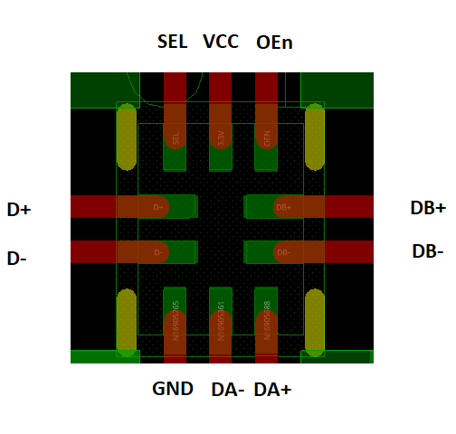
GUID-20220805-SS0I-N4ZT-VDQG-T2WQ0QCFN14C-low.png Figure 8-7 TMUXHS221LV Layout Example