ZHCSN19A December 2020 – October 2024 TMUXHS4412
PRODUCTION DATA
- 1
- 1 特性
- 2 应用
- 3 说明
- 4 Pin Configuration and Functions
- 5 Specifications
- 6 Detailed Description
- 7 Application and Implementation
- 8 Device and Documentation Support
- 9 Revision History
- 10Mechanical, Packaging, and Orderable Information
7.1 Application Information
The TMUXHS4412 is an analog 4-channel high-speed mux/demux type of switch that can be used for routing high-speed signals between two different locations on a circuit board. The TMUXHS4412 can be used for many high-speed interfaces including:
- Peripheral Component Interconnect Express (PCIe) Gen 1.0, 2.0, 3.0, 4.0
- USB 4.0
- Universal Serial Bus (USB) 3.2 Gen 1.0, 2.0
- Serial ATA (SATA/eSATA)
- Serial Attached SCSI (SAS)
- Display Port (DP) 1.4, 2.0
- Thunderbolt (TBT) 3.0
- MIPI Camera Serial Interface (CSI-2), Display Serial Interface (DSI)
- Low Voltage Differential Signaling (LVDS)
- Serdes Framer Interface (SFI)
- Ethenet Interfaces
The mux/demux selection pin SEL can easily be controlled by an available GPIO pin of a controller or hard tie to voltage level H or L as an application requires.
The TMUXHS4412 with adaptive voltage tracking technology can support applications where the common mode is different between the RX and TX pair. The switch paths of the TMUXHS4412 have internal weak pulldown resistors of 1MΩ on the common port pins. While these resistors biases the device data channels to common-mode voltage (CMV) of 0V with a weak strength, TI recommends to bias the device from either side of the device to a valid value (in the range of 0V to 1.8V in 3.3V supply voltage mode). It is expected that the system/host controller and device/end point common-mode bias impedances are much stronger (smaller) than the TMUXHS4412 internal pulldown resistors and are therefore not impacted.
Many interfaces require AC coupling between the transmitter and receiver. The 0201 or 0402 capacitors are the preferred option to provide AC coupling. Avoid the 0603, 0805 size capacitors and C-packs. When placing AC-coupling capacitors, symmetric placement is best. The capacitor value must be chosen according to the specific interface the device is being used. Make sure the value of the capacitor matches the positive and negative signal pair. For many interfaces such as USB 3.2 and PCIe, the designer can place them along the TX pairs on the system board, which are usually routed on the top layer of the board. Use the appropriate value for AC-coupling capacitors based on the application and interface specifications.
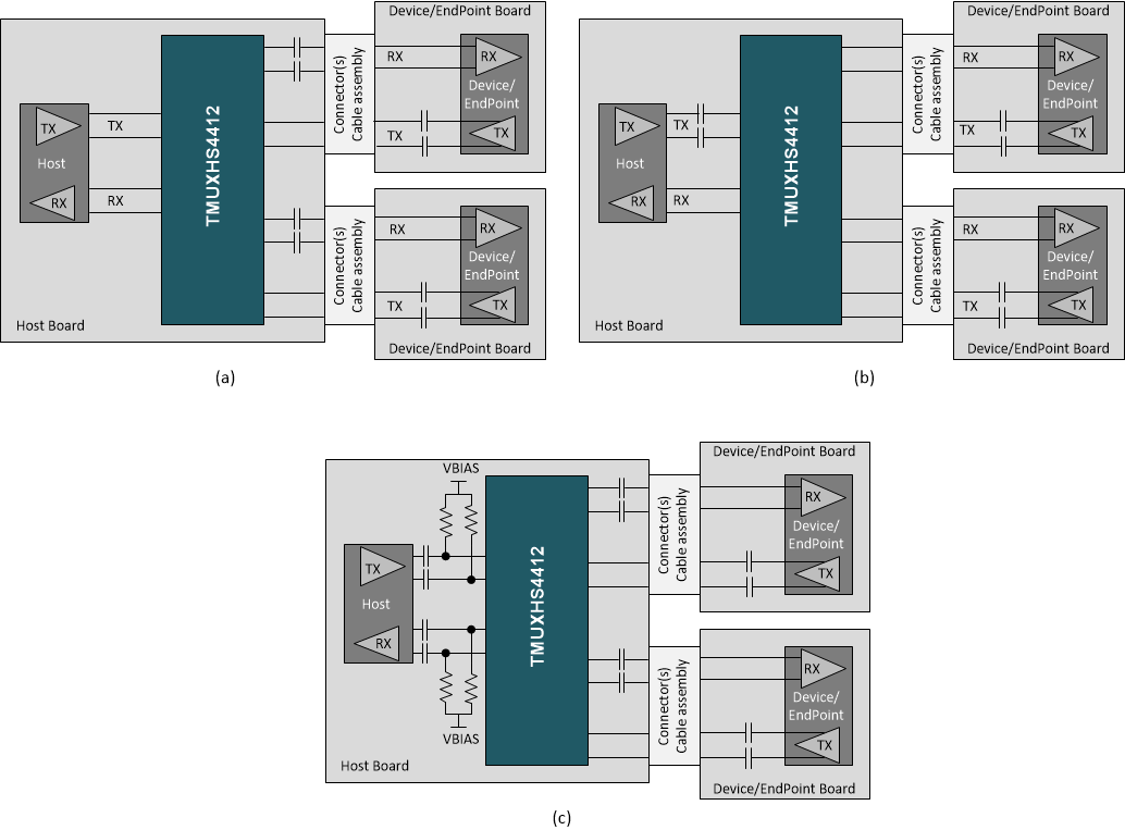
The AC-coupling capacitors have several placement options. Typical use cases warrant that the capacitors are placed on one side of the TMUXHS4412. In certain use cases, if both sides of the TMUXHS4412 is AC-coupled, TI recommends to use appropriate CMV biasing for the device. 10kΩ to GND or any other bias voltage in the valid CMV range for each D[0/1/2/3][P/N] pin of the common port suffice for most use cases. Figure 7-1 shows a few placement options. Note for brevity not all channels are illustrated in the block diagrams. Some interfaces such as USB SS and PCIe recommend placing AC-coupling capacitors on the TX signals before a connector. Option (a) features TX AC-coupling capacitors on the connector side of the TMUXHS4412. Option (b) illustrates the capacitors on the host of the TMUXHS4412. Option (c) showcases where the TMUXHS4412 is AC-coupled on both sides. VBIAS must be within the valid CMV of the device.
 Figure 7-1 AC-Coupling Capacitors Placement Options Between Host and Device / Endpoint