SLOS369G July   2002  – October 2015 TPA2005D1

PRODUCTION DATA.  

  1. Features
  2. Applications
  3. Description
  4. Revision History
  5. Device Comparison Table
  6. Pin Configuration and Functions
  7. Specifications
    1. 7.1 Absolute Maximum Ratings
    2. 7.2 ESD Ratings
    3. 7.3 Recommended Operating Conditions
    4. 7.4 Thermal Information
    5. 7.5 Electrical Characteristics
    6. 7.6 Operating Characteristics
    7. 7.7 Typical Characteristics
  8. Parameter Measurement Information
  9. Detailed Description
    1. 9.1 Overview
    2. 9.2 Functional Block Diagram
    3. 9.3 Feature Description
      1. 9.3.1 Fully Differential Amplifier
        1. 9.3.1.1 Advantages of Fully Differential Amplifiers
      2. 9.3.2 Efficiency and Thermal Information
      3. 9.3.3 Eliminating the Output Filter with the TPA2005D1
        1. 9.3.3.1 Effect on Audio
        2. 9.3.3.2 Traditional Class-D Modulation Scheme
        3. 9.3.3.3 TPA2005D1 Modulation Scheme
        4. 9.3.3.4 Efficiency: Why You Must Use a Filter With the Traditional Class-D Modulation Scheme
        5. 9.3.3.5 Effects of Applying a Square Wave Into a Speaker
        6. 9.3.3.6 When to Use an Output Filter
      4. 9.3.4 Thermal and Short-Circuit Protection
    4. 9.4 Device Functional Modes
      1. 9.4.1 Summing Input Signals with the TPA2005D1
        1. 9.4.1.1 Summing Two Differential Input Signals
        2. 9.4.1.2 Summing a Differential Input Signal and a Single-Ended Input Signal
        3. 9.4.1.3 Summing Two Single-Ended Input Signals
      2. 9.4.2 Shutdown Mode
  10. 10Application and Implementation
    1. 10.1 Application Information
    2. 10.2 Typical Applications
      1. 10.2.1 TPA2005D1 with Differential Input
        1. 10.2.1.1 Design Requirements
        2. 10.2.1.2 Detailed Design Procedure
          1. 10.2.1.2.1 Component Selection
          2. 10.2.1.2.2 Input Resistors (RI)
          3. 10.2.1.2.3 Decoupling Capacitor (CS)
        3. 10.2.1.3 Application Curves
      2. 10.2.2 TPA2005D1 with Differential Input and Input Capacitors
        1. 10.2.2.1 Design Requirements
        2. 10.2.2.2 Detailed Design Procedure
          1. 10.2.2.2.1 Input Capacitors (CI)
      3. 10.2.3 TPA2005D1 with Single-Ended Input
        1. 10.2.3.1 Design Requirements
        2. 10.2.3.2 Detailed Design Procedure
  11. 11Power Supply Recommendations
    1. 11.1 Power Supply Decoupling Capacitors
  12. 12Layout
    1. 12.1 Layout Guidelines
      1. 12.1.1 Component Location
      2. 12.1.2 Trace Width
      3. 12.1.3 MicroStar Junior™ BGA Specifications
    2. 12.2 Layout Examples
  13. 13Device and Documentation Support
    1. 13.1 Community Resources
    2. 13.2 Trademarks
    3. 13.3 Electrostatic Discharge Caution
    4. 13.4 Glossary
  14. 14Mechanical, Packaging, and Orderable Information

封装选项

请参考 PDF 数据表获取器件具体的封装图。

机械数据 (封装 | 引脚)
  • DGN|8
  • DRB|8
散热焊盘机械数据 (封装 | 引脚)
订购信息

12 Layout

12.1 Layout Guidelines

12.1.1 Component Location

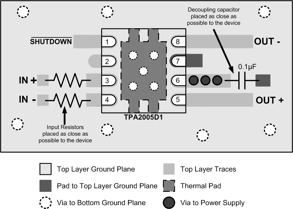
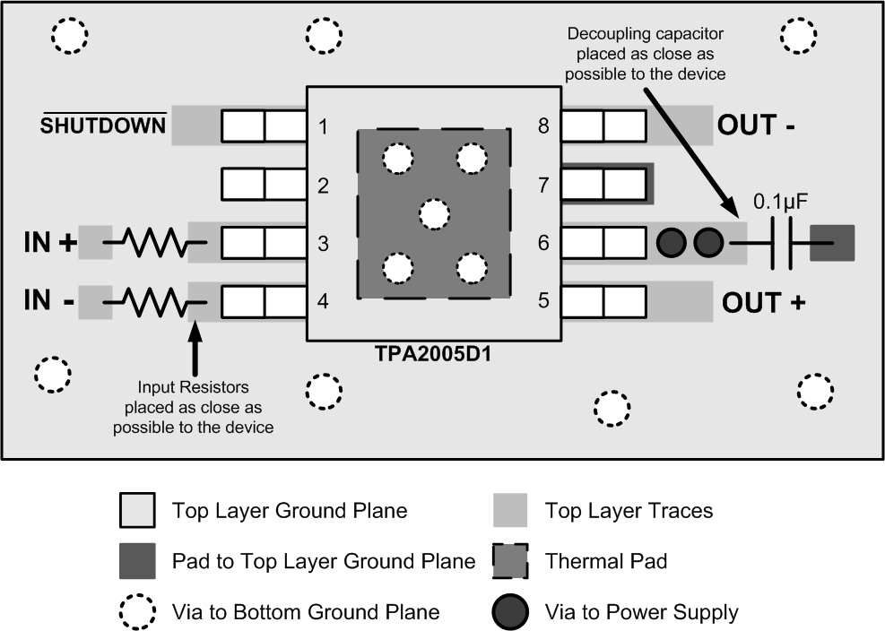
Place all the external components close to the TPA2005D1. The input resistors need to be close to the TPA2005D1 input pins so noise does not couple on the high impedance nodes between the input resistors and the input amplifier of the TPA2005D1. Placing the decoupling capacitor, CS, close to the TPA2005D1 is important for the efficiency of the class-D amplifier. Any resistance or inductance in the trace between the device and the capacitor can cause a loss in efficiency.

12.1.2 Trace Width

Make the high current traces going to pins VDD, GND, VO+ and VO- of the TPA2005D1 have a minimum width of 0,7 mm. If these traces are too thin, the TPA2005D1's performance and output power will decrease. The input traces do not need to be wide, but do need to run side-by-side to enable common-mode noise cancellation.

12.1.3 MicroStar Junior™ BGA Specifications

Use the following MicroStar Junior BGA ball diameters:

  • 0,25 mm diameter solder mask
  • 0,28 mm diameter solder paste mask/stencil
  • 0,38 mm diameter copper trace

Figure 44 shows how to lay out a board for the TPA2005D1 MicroStar Junior BGA.
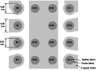
TPA2005D1 ai_BGA_BL_los369.gif Figure 44. TPA2005D1 MicroStar Junior BGA Board Layout (Top View)
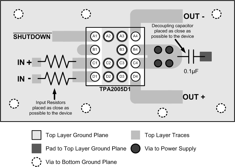
12.2 Layout Examples

TPA2005D1 layout_BGA.gif Figure 45. TPA2005D1 MicroStar Junior™ BGA Package Layout Example
TPA2005D1 layout_QFN.gif Figure 46. TPA2005D1 DRB Package Layout Example
TPA2005D1 layout_MSOP.gif Figure 47. TPA2005D1 DGN Package Layout Example