ZHCSFV8C May 2016 – January 2018 TPA3128D2 , TPA3129D2
PRODUCTION DATA.
- 1 特性
- 2 应用
- 3 说明
- 4 Revision History
- 5 Pin Configuration and Functions
- 6 Specifications
-
7 Detailed Description
- 7.1 Overview
- 7.2 Functional Block Diagram
- 7.3
Feature Description
- 7.3.1 Gain Setting and Master and Slave
- 7.3.2 Input Impedance
- 7.3.3 Startup and Shutdown Operation
- 7.3.4 PLIMIT Operation
- 7.3.5 GVDD Supply
- 7.3.6 BSPx AND BSNx Capacitors
- 7.3.7 Differential Inputs
- 7.3.8 Device Protection System
- 7.3.9 DC Detect Protection
- 7.3.10 Short-Circuit Protection and Automatic Recovery Feature
- 7.3.11 Thermal Protection
- 7.3.12 Device Modulation Scheme
- 7.3.13 Efficiency: LC Filter Required with the Traditional Class-D Modulation Scheme
- 7.3.14 Ferrite Bead Filter Considerations
- 7.3.15 When to Use an Output Filter for EMI Suppression
- 7.3.16 AM Avoidance EMI Reduction
- 7.4 Device Functional Modes
- 8 Applications and Implementation
- 9 Power Supply Recommendations
- 10Layout
- 11器件和文档支持
- 12机械、封装和可订购信息
7.3.1 Gain Setting and Master and Slave
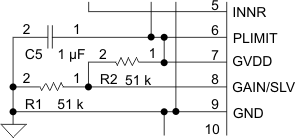
The gain of the TPA312xD2 is set by the voltage divider connected to the GAIN/SLV control pin. Master or Slave mode is also controlled by the same pin. An internal ADC is used to detect the 8 input states. The first four stages sets the GAIN in Master mode in gains of 20, 26, 32, 36 dB respectively, while the next four stages sets the GAIN in Slave mode in gains of 20, 26, 32, 36 dB respectively. The gain setting is latched during power-up and cannot be changed while device is powered. Table 1 lists the recommended resistor values and the state and gain:
Table 1. Gain and Master/Slave
| MASTER / SLAVE MODE | GAIN | R1 (to GND)(1) | R2 (to GVDD)(1) | INPUT IMPEDANCE |
|---|---|---|---|---|
| Master | 20 dB | 5.6 kΩ | OPEN | 60 kΩ |
| Master | 26 dB | 20 kΩ | 100 kΩ | 30 kΩ |
| Master | 32 dB | 39 kΩ | 100 kΩ | 15 kΩ |
| Master | 36 dB | 47 kΩ | 75 kΩ | 9 kΩ |
| Slave | 20 dB | 51 kΩ | 51 kΩ | 60 kΩ |
| Slave | 26 dB | 75 kΩ | 47 kΩ | 30 kΩ |
| Slave | 32 dB | 100 kΩ | 39 kΩ | 15 kΩ |
| Slave | 36 dB | 100 kΩ | 16 kΩ | 9 kΩ |
 Figure 25. Gain, Master/Slave
In Master mode, SYNC terminal is an output, in Slave mode, SYNC terminal is an input for a clock input. TTL logic levels with compliance to GVDD.