ZHCSH28B September 2017 – December 2017 TPA3221
PRODUCTION DATA.
- 1 特性
- 2 应用
- 3 说明
- 4 修订历史记录
- 5 Device Comparison Table
- 6 Pin Configuration and Functions
-
7 Specifications
- 7.1 Absolute Maximum Ratings
- 7.2 ESD Ratings
- 7.3 Recommended Operating Conditions
- 7.4 Thermal Information
- 7.5 Electrical Characteristics
- 7.6 Audio Characteristics (BTL)
- 7.7 Audio Characteristics (PBTL)
- 7.8 Typical Characteristics, BTL Configuration, AD-mode
- 7.9 Typical Characteristics, PBTL Configuration, AD-mode
- 8 Parameter Measurement Information
-
9 Detailed Description
- 9.1 Overview
- 9.2 Functional Block Diagrams
- 9.3 Feature Description
- 9.4
Device Functional Modes
- 9.4.1 Powering Up
- 9.4.2 Powering Down
- 9.4.3 Device Reset
- 9.4.4 Device Soft Mute
- 9.4.5
Device Protection System
- 9.4.5.1 Overload and Short Circuit Current Protection
- 9.4.5.2 Signal Clipping and Pulse Injector
- 9.4.5.3 DC Speaker Protection
- 9.4.5.4 Pin-to-Pin Short Circuit Protection (PPSC)
- 9.4.5.5 Overtemperature Protection OTW and OTE
- 9.4.5.6 Undervoltage Protection (UVP), Overvoltage Protection (OVP) and Power-on Reset (POR)
- 9.4.5.7 Fault Handling
- 10Application and Implementation
- 11Power Supply Recommendations
- 12Layout
- 13器件和文档支持
- 14机械、封装和可订购信息
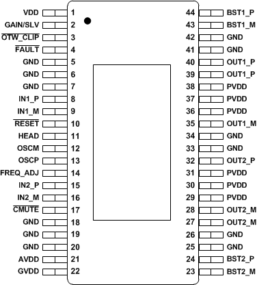
6 Pin Configuration and Functions
The TPA3221 is available in a thermally enhanced TSSOP package.
The package type contains a heat slug that is located on the top side of the device for convenient thermal coupling to the heat sink.
DDV Package
HTSSOP 44-Pin
(Top View)

Pin Functions
| NAME | NO. | I/O | DESCRIPTION |
|---|---|---|---|
| HEAD | 11 | I | 0 = AD, 1 = HEAD. Refer to: AD-Mode and HEAD-Mode PWM Modulation |
| AVDD | 21 | P | AVDD voltage supply. Refer to: Internal LDO, AVDD and GVDD Supplies |
| BST1_M | 43 | P | OUT1_M HS bootstrap supply (BST), 0.033 μF capacitor to OUT1_M required.
Refer to: BST capacitors |
| BST1_P | 44 | P | OUT1_P HS bootstrap supply (BST), 0.033 μF capacitor to OUT1_P required.
Refer to: BST capacitors |
| BST2_M | 23 | P | OUT2_M HS bootstrap supply (BST), 0.033 μF capacitor to OUT2_M required.
Refer to: BST capacitors |
| BST2_P | 24 | P | OUT2_P HS bootstrap supply (BST), 0.033 μF capacitor to OUT2_P required.
Refer to: BST capacitors |
| CMUTE | 17 | P | Mute and Startup Timing Capacitor. Connect a 33 nF capacitor to GND. Refer to: Device Reset |
| FAULT | 4 | O | Shutdown signal, open drain; active low. Refer to: Error Reporting |
| FREQ_ADJ | 14 | O | Oscillator frequency programming pin. Refer to: Oscillator |
| GAIN/SLV | 2 | I | Closed loop gain and master/slave programming pin.
Refer to: Input Configuration, Gain Setting And Master / Slave Operation |
| GND | 5, 6, 7, 18, 19, 20, 25, 26, 33, 34, 41, 42 | P | Ground |
| GVDD | 22 | P | Gate drive supply. Refer to: Internal LDO, AVDD and GVDD Supplies |
| IN1_M | 9 | I | Negative audio input for channel 1 |
| IN1_P | 8 | I | Positive audio input for channel 1 |
| IN2_M | 16 | I | Negative audio input for channel 2 |
| IN2_P | 15 | I | Positive audio input for channel 2 |
| OSCM | 12 | I/O | Oscillator synchronization interface.
Refer to: Input Configuration, Gain Setting And Master / Slave Operation |
| OSCP | 13 | I/O | Oscillator synchronization interface.
Refer to: Input Configuration, Gain Setting And Master / Slave Operation |
| OTW_CLIP | 3 | O | Clipping warning and Over-temperature warning; open drain; active low.
Refer to: Error Reporting |
| OUT1_M | 35 | O | Negative output for channel 1 |
| OUT1_P | 39, 40 | O | Positive output for channel 1 |
| OUT2_M | 27, 28 | O | Negative output for channel 2 |
| OUT2_P | 32 | O | Positive output for channel 2 |
| PVDD | 29, 30, 31, 36, 37, 38 | P | PVDD supply. Refer to: PVDD Capacitor Recommendation, PVDD Supply |
| RESET | 10 | I | Device reset Input; active low. Refer to: Fault Handling, Powering Up, Powering Down |
| VDD | 1 | P | Input power supply. Refer to: Internal LDO, VDD Supply |
| PowerPad™ | P | Ground, connect to grounded heatsink. Placed on top side of device. |
Table 1. Mode Selection Pins
| MODE PINS(2) | INPUT MODE(1) | OUTPUT CONFIGURATION | DESCRIPTION | ||||
|---|---|---|---|---|---|---|---|
| IN2_M | IN2_P | HEAD | |||||
| X | X | 0 | 1N/2N + 1 | 2 × BTL | Stereo, BTL output configuration, AD mode modulation | ||
| X | X | 1 | 1N/2N + 1 | 2 × BTL | Stereo, BTL output configuration, HEAD mode modulation | ||
| 0 | 0 | 0 | 1N/2N + 1 | 1 x PBTL | Mono, Parallelled BTL configuration. Connect OUT1_P to OUT2_P and OUT1_M to OUT2_M, AD mode modulation | ||
| 0 | 0 | 1 | 1N/2N + 1 | 1 x PBTL | Mono, Parallelled BTL configuration. Connect OUT1_P to OUT2_P and OUT1_M to OUT2_M, HEAD mode modulation | ||
| 1 | 1 | 0 | 1N/2N + 1 | 1 x BTL | Mono, BTL configuration. OUT1_M and OUT1_P active, AD mode modulation | ||
| 1 | 1 | 1 | 1N/2N + 1 | 1 x BTL | Mono, BTL configuration. OUT1_M and OUT1_P active, HEAD mode modulation | ||
(1) 2N refers to differential input signal, 1N refers to single ended input signal. +1 refers to number of logic control (RESET) input pins.
(2) X refers to inputs connected through AC coupling capacitor, 0 refers to logic low (GND), 1 refers to logic high (AVDD).