ZHCSH28B September 2017 – December 2017 TPA3221
PRODUCTION DATA.
- 1 特性
- 2 应用
- 3 说明
- 4 修订历史记录
- 5 Device Comparison Table
- 6 Pin Configuration and Functions
-
7 Specifications
- 7.1 Absolute Maximum Ratings
- 7.2 ESD Ratings
- 7.3 Recommended Operating Conditions
- 7.4 Thermal Information
- 7.5 Electrical Characteristics
- 7.6 Audio Characteristics (BTL)
- 7.7 Audio Characteristics (PBTL)
- 7.8 Typical Characteristics, BTL Configuration, AD-mode
- 7.9 Typical Characteristics, PBTL Configuration, AD-mode
- 8 Parameter Measurement Information
-
9 Detailed Description
- 9.1 Overview
- 9.2 Functional Block Diagrams
- 9.3 Feature Description
- 9.4
Device Functional Modes
- 9.4.1 Powering Up
- 9.4.2 Powering Down
- 9.4.3 Device Reset
- 9.4.4 Device Soft Mute
- 9.4.5
Device Protection System
- 9.4.5.1 Overload and Short Circuit Current Protection
- 9.4.5.2 Signal Clipping and Pulse Injector
- 9.4.5.3 DC Speaker Protection
- 9.4.5.4 Pin-to-Pin Short Circuit Protection (PPSC)
- 9.4.5.5 Overtemperature Protection OTW and OTE
- 9.4.5.6 Undervoltage Protection (UVP), Overvoltage Protection (OVP) and Power-on Reset (POR)
- 9.4.5.7 Fault Handling
- 10Application and Implementation
- 11Power Supply Recommendations
- 12Layout
- 13器件和文档支持
- 14机械、封装和可订购信息
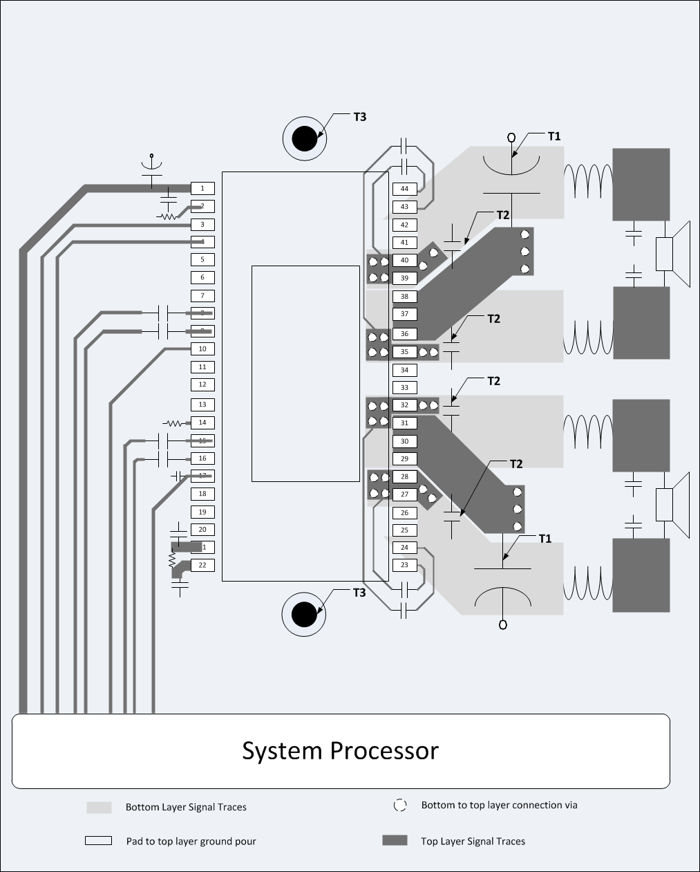
12.2.1 BTL Application Printed Circuit Board Layout Example

A. Note: PCB layout example shows composite layout. Dark grey: Top layer copper traces, light gray: Bottom layer copper traces. All PCB area not used for traces should be GND copper pour (transparent on example image)
B. Note T1: PVDD decoupling bulk capacitors should be as close as possible to the PVDD and GND_X pins, the heat sink sets the distance. Wide traces should be routed on the top layer with direct connection to the pins and without going through vias. No vias or traces should be blocking the current path.
C. Note T2: Close decoupling of PVDD with low impedance X7R ceramic capacitors is placed under the heat sink and close to the pins.
D. Note T3: Heat sink needs to have a good connection to PCB ground.
Figure 53. BTL Application Printed Circuit Board - Composite