ZHCSFM5A September 2016 – October 2016 TPA3245
PRODUCTION DATA.
- 1 特性
- 2 应用
- 3 说明
- 4 修订历史记录
- 5 Device Comparison Table
- 6 Pin Configuration and Functions
-
7 Specifications
- 7.1 Absolute Maximum Ratings
- 7.2 ESD Ratings
- 7.3 Recommended Operating Conditions
- 7.4 Thermal Information
- 7.5 Electrical Characteristics
- 7.6 Audio Characteristics (BTL)
- 7.7 Audio Characteristics (SE)
- 7.8 Audio Characteristics (PBTL)
- 7.9 Typical Characteristics, BTL Configuration
- 7.10 Typical Characteristics, SE Configuration
- 7.11 Typical Characteristics, PBTL Configuration
- 8 Parameter Measurement Information
-
9 Detailed Description
- 9.1 Overview
- 9.2 Functional Block Diagrams
- 9.3 Feature Description
- 9.4
Device Protection System
- 9.4.1 Overload and Short Circuit Current Protection
- 9.4.2 Signal Clipping and Pulse Injector
- 9.4.3 DC Speaker Protection
- 9.4.4 Pin-to-Pin Short Circuit Protection (PPSC)
- 9.4.5 Overtemperature Protection OTW and OTE
- 9.4.6 Undervoltage Protection (UVP) and Power-on Reset (POR)
- 9.4.7 Fault Handling
- 9.4.8 Device Reset
-
10Application and Implementation
- 10.1 Application Information
- 10.2 Typical Applications
- 11Power Supply Recommendations
-
12Layout
- 12.1 Layout Guidelines
- 12.2
Layout Examples
- 12.2.1 BTL Application Printed Circuit Board Layout Example
- 12.2.2 SE Application Printed Circuit Board Layout Example
- 12.2.3 PBTL (Outputs Paralleled before LC filter) Application Printed Circuit Board Layout Example
- 12.2.4 PBTL (Outputs Paralleled after LC filter) Application Printed Circuit Board Layout Example
- 13器件和文档支持
- 14机械、封装和可订购信息
7 Specifications
7.1 Absolute Maximum Ratings
over operating free-air temperature range (unless otherwise noted) (1)| MIN | MAX | UNIT | ||
|---|---|---|---|---|
| Supply voltage | BST_X to GVDD_X(2) | –0.3 | 43 | V |
| VDD to GND | –0.3 | 13.2 | V | |
| GVDD_X to GND(2) | –0.3 | 13.2 | V | |
| PVDD_X to GND(2) | –0.3 | 43 | V | |
| DVDD to GND | –0.3 | 4.2 | V | |
| AVDD to GND | –0.3 | 8.5 | V | |
| VBG to GND | -0.3 | 4.2 | V | |
| Interface pins | OUT_X to GND(2) | –0.3 | 43 | V |
| BST_X to GND(2) | –0.3 | 55.5 | V | |
| OC_ADJ, M1, M2, OSC_IOP, OSC_IOM, FREQ_ADJ, C_START, to GND | –0.3 | 4.2 | V | |
| RESET, FAULT, CLIP_OTW to GND | –0.3 | 4.2 | V | |
| INPUT_X to GND | –0.3 | 7 | V | |
| Continuous sink current, RESET, FAULT, CLIP_OTW to GND | 9 | mA | ||
| TJ | Operating junction temperature range | 0 | 150 | °C |
| Tstg | Storage temperature range | –40 | 150 | °C |
(1) Stresses beyond those listed under Absolute Maximum Ratings may cause permanent damage to the device. These are stress ratings only, which do not imply functional operation of the device at these or any other conditions beyond those indicated under Recommended Operating Conditions. Exposure to absolute-maximum-rated conditions for extended periods may affect device reliability.
(2) These voltages represents the DC voltage + peak AC waveform measured at the terminal of the device in all conditions.
7.2 ESD Ratings
| VALUE | UNIT | |||
|---|---|---|---|---|
| VESD | Electrostatic discharge | Human body model (HBM), per ANSI/ESDA/JEDEC JS-001, all pins (1) | ±1000 | V |
| Charged device model (CDM), per JEDEC specification JESD22-C101, all pins(2) | ±250 | V | ||
(1) JEDEC document JEP155 states that 500-V HBM allows safe manufacturing with a standard ESD control process.
(2) JEDEC document JEP157 states that 250-V CDM allows safe manufacturing with a standard ESD control process.
7.3 Recommended Operating Conditions
over operating free-air temperature range (unless otherwise noted)| MIN | TYP | MAX | UNIT | |||
|---|---|---|---|---|---|---|
| PVDD_x | Half-bridge supply | DC supply voltage | 12 | 30 | 31.5 | V |
| GVDD_x | Supply for logic regulators and gate-drive circuitry | DC supply voltage | 10.8 | 12 | 13.2 | V |
| VDD | Digital regulator supply voltage | DC supply voltage | 10.8 | 12 | 13.2 | V |
| RL(BTL) | Load impedance | Output filter inductance within recommended value range | 2.7 | 4 | Ω | |
| RL(SE) | 1.5 | 3 | ||||
| RL(PBTL) | 1.6 | 2 | ||||
| LOUT(BTL) | Output filter inductance | Minimum output inductance at IOC | 5 | μH | ||
| LOUT(SE) | 5 | |||||
| LOUT(PBTL) | 5 | |||||
| FPWM | PWM frame rate selectable for AM interference avoidance; 1% Resistor tolerance | Nominal | 575 | 600 | 625 | kHz |
| AM1 | 475 | 500 | 525 | |||
| AM2 | 430 | 450 | 470 | |||
| R(FREQ_ADJ) | PWM frame rate programming resistor | Nominal; Master mode | 9.9 | 10 | 10.1 | kΩ |
| AM1; Master mode | 19.8 | 20 | 20.2 | |||
| AM2; Master mode | 29.7 | 30 | 30.3 | |||
| CPVDD | PVDD close decoupling capacitors | 1.0 | μF | |||
| ROC | Over-current programming resistor | Resistor tolerance = 5% | 22 | 30 | kΩ | |
| ROC(LATCHED) | Over-current programming resistor | Resistor tolerance = 5% | 47 | 64 | kΩ | |
| V(FREQ_ADJ) | Voltage on FREQ_ADJ pin for slave mode operation | Slave mode | 3.3 | V | ||
| TJ | Junction temperature | 0 | 125 | °C | ||
7.4 Thermal Information
| THERMAL METRIC(1) | TPA3251D2 | UNIT | ||
|---|---|---|---|---|
| DDV 44-PINS HTSSOP | ||||
| FIXED 85°C HEATSINK TEMPERATURE(2) | ||||
| RθJA | Junction-to-ambient thermal resistance | 2.8(2) | °C/W | |
| RθJC(top) | Junction-to-case (top) thermal resistance | 0.5 | ||
| RθJB | Junction-to-board thermal resistance | n/a | ||
| ψJT | Junction-to-top characterization parameter | 0.9 | ||
| ψJB | Junction-to-board characterization parameter | n/a | ||
| RθJC(bot) | Junction-to-case (bottom) thermal resistance | n/a | ||
(1) For more information about traditional and new thermal metrics, see the Semiconductor and IC Package Thermal Metrics application report.
(2) Thermal data are obtained with 85°C heat sink temperature using thermal compound with 0.7W/mK thermal conductivity and 2mil thickness. In this model heat sink temperature is considered to be the ambient temperature and only path for dissipation is to the heatsink.
7.5 Electrical Characteristics
PVDD_X = 30 V, GVDD_X = 12 V, VDD = 12 V, TC (Case temperature) = 75°C, fS = 600 kHz, unless otherwise specified.| PARAMETER | TEST CONDITIONS | MIN | TYP | MAX | UNIT | |
|---|---|---|---|---|---|---|
| INTERNAL VOLTAGE REGULATOR AND CURRENT CONSUMPTION | ||||||
| DVDD | Voltage regulator, only used as reference node | VDD = 12 V | 3.3 | V | ||
| AVDD | Voltage regulator, only used as reference node | VDD = 12 V | 7.8 | V | ||
| IVDD | VDD supply current | Operating, 50% duty cycle | 40 | mA | ||
| Idle, reset mode | 10 | |||||
| IGVDD_X | Gate-supply current per full-bridge | 50% duty cycle | 19 | mA | ||
| Reset mode | 2.5 | |||||
| IPVDD_X | PVDD idle current per full bridge | 50% duty cycle with recommended output filter | 15 | mA | ||
| Reset mode, No switching | 1.1 | mA | ||||
| ANALOG INPUTS | ||||||
| RIN | Input resistance | 24 | kΩ | |||
| VIN | Maximum input voltage swing | 7 | V | |||
| IIN | Maximum input current | 1 | mA | |||
| G | Inverting voltage Gain | VOUT/VIN | 18 | dB | ||
| OSCILLATOR | ||||||
| fOSC(IO+) (1) | Nominal, Master Mode | FPWM × 6 | 3.45 | 3.6 | 3.75 | MHz |
| AM1, Master Mode | 2.85 | 3 | 3.15 | |||
| AM2, Master Mode | 2.58 | 2.7 | 2.82 | |||
| VIH | High level input voltage | 1.86 | V | |||
| VIL | Low level input voltage | 1.45 | V | |||
| OUTPUT-STAGE MOSFETs | ||||||
| RDS(on) | Drain-to-source resistance, low side (LS) | TJ = 25°C, Includes metallization resistance, GVDD = 12 V |
65 | mΩ | ||
| Drain-to-source resistance, high side (HS) | 65 | mΩ | ||||
| I/O PROTECTION | ||||||
| Vuvp,VDD,GVDD | Undervoltage protection limit, GVDD_x and VDD | 8.6 | V | |||
| Vuvp,VDD, GVDD,hyst (2) | 0.85 | V | ||||
| Vuvp,PVDD | Undervoltage protection limit, PVDD_x | 9.7 | V | |||
| Vuvp,PVDD,hyst (2) | 1.25 | V | ||||
| OTW | Overtemperature warning, CLIP_OTW(2) | 115 | 125 | 135 | °C | |
| OTWhyst (2) | Temperature drop needed below OTW temperature for CLIP_OTW to be inactive after OTW event. | 20 | °C | |||
| OTE(2) | Overtemperature error | 145 | 155 | 165 | °C | |
| OTEhyst (2) | A reset needs to occur for FAULT to be released following an OTE event | 20 | °C | |||
| OTE-OTW(differential) (2) | OTE-OTW differential | 30 | °C | |||
| OLPC | Overload protection counter | fPWM = 600 kHz (1024 PWM cycles) | 1.7 | ms | ||
| IOC | Overcurrent limit protection | Resistor – programmable, nominal peak current in 1Ω load, ROCP = 22 kΩ | 13.5 | A | ||
| IOC(LATCHED) | Overcurrent limit protection | Resistor – programmable, peak current in 1Ω load, ROCP = 47kΩ | 13.5 | A | ||
| IDCspkr | DC Speaker Protection Current Threshold | BTL current imbalance threshold | 2 | A | ||
| IOCT | Overcurrent response time | Time from switching transition to flip-state induced by overcurrent. | 150 | ns | ||
| IPD | Output pulldown current of each half | Connected when RESET is active to provide bootstrap charge. Not used in SE mode. | 3 | mA | ||
| STATIC DIGITAL SPECIFICATIONS | ||||||
| VIH | High level input voltage | M1, M2, OSC_IOP, OSC_IOM, RESET | 1.9 | V | ||
| VIL | Low level input voltage | 0.8 | V | |||
| Ilkg | Input leakage current | 100 | μA | |||
| OTW/SHUTDOWN (FAULT) | ||||||
| RINT_PU | Internal pullup resistance, CLIP_OTW to DVDD, FAULT to DVDD | 20 | 26 | 32 | kΩ | |
| VOH | High level output voltage | Internal pullup resistor | 3 | 3.3 | 3.6 | V |
| VOL | Low level output voltage | IO = 4 mA | 200 | 500 | mV | |
| Device fanout | CLIP_OTW, FAULT | No external pullup | 30 | devices | ||
(1) Nominal, AM1 and AM2 use same internal oscillator with fixed ratio 6 : 5 : 4.5
(2) Specified by design.
7.6 Audio Characteristics (BTL)
PCB and system configuration are in accordance with recommended guidelines. Audio frequency = 1 kHz, PVDD_X = 30 V, GVDD_X = 12 V, RL = 4 Ω, fS = 600 kHz, ROC = 22 kΩ, TC = 75°C, Output Filter: LDEM = 10 μH, CDEM = 1 µF, mode = 00, AES17 + AUX-0025 measurement filters,unless otherwise noted.| PARAMETER | TEST CONDITIONS | MIN | TYP | MAX | UNIT | |
|---|---|---|---|---|---|---|
| PO | Power output per channel | RL = 3 Ω, 10% THD+N | 145 | W | ||
| RL = 4 Ω, 10% THD+N | 115 | |||||
| RL = 3 Ω, 1% THD+N | 115 | |||||
| RL = 4 Ω, 1% THD+N | 95 | |||||
| THD+N | Total harmonic distortion + noise | 1 W | 0.005% | |||
| Vn | Output integrated noise | A-weighted, AES17 filter, Input Capacitor Grounded | 50 | μV | ||
| |VOS| | Output offset voltage | Inputs AC coupled to GND | 20 | 60 | mV | |
| SNR | Signal-to-noise ratio(1) | 112 | dB | |||
| DNR | Dynamic range | 113 | dB | |||
| Pidle | Power dissipation due to Idle losses (IPVDD_X) | PO = 0, 4 channels switching(2) | 0.45 | W | ||
(1) SNR is calculated relative to 1% THD+N output level.
(2) Actual system idle losses also are affected by core losses of output inductors.
7.7 Audio Characteristics (SE)
PCB and system configuration are in accordance with recommended guidelines. Audio frequency = 1 kHz, PVDD_X = 30 V, GVDD_X = 12 V, RL = 2 Ω, fS = 600 kHz, ROC = 22 kΩ, TC = 75°C, Output Filter: LDEM = 15 μH, CDEM = 680 nF, MODE = 11, AES17 + AUX-0025 measurement filters, unless otherwise noted.| PARAMETER | TEST CONDITIONS | MIN | TYP | MAX | UNIT | |
|---|---|---|---|---|---|---|
| PO | Power output per channel | RL = 2 Ω, 10% THD+N | 55 | W | ||
| RL = 3 Ω, 10% THD+N | 39 | |||||
| RL = 4 Ω, 10% THD+N | 30 | |||||
| RL = 2 Ω, 1% THD+N | 44 | |||||
| RL = 3 Ω, 1% THD+N | 32 | |||||
| RL = 4 Ω, 1% THD+N | 25 | |||||
| THD+N | Total harmonic distortion + noise | 1 W | 0.01% | |||
| Vn | Output integrated noise | A-weighted, AES17 filter, Input Capacitor Grounded | 100 | μV | ||
| SNR | Signal to noise ratio(1) | A-weighted | 106 | dB | ||
| DNR | Dynamic range | A-weighted | 101 | dB | ||
| Pidle | Power dissipation due to idle losses (IPVDD_X) | PO = 0, 4 channels switching(2) | 0.45 | W | ||
(1) SNR is calculated relative to 1% THD+N output level.
(2) Actual system idle losses are affected by core losses of output inductors.
7.8 Audio Characteristics (PBTL)
PCB and system configuration are in accordance with recommended guidelines. Audio frequency = 1 kHz, PVDD_X = 30 V, GVDD_X = 12 V, RL = 2 Ω, fS = 600 kHz, ROC = 22 kΩ, TC = 75°C, Output Filter: LDEM = 10 μH, CDEM = 1 µF, MODE = 10, outputs paralleled before LC filter, AES17 + AUX-0025 measurement filters, unless otherwise noted.| PARAMETER | TEST CONDITIONS | MIN | TYP | MAX | UNIT | |
|---|---|---|---|---|---|---|
| PO | Power output per channel | RL = 2 Ω, 10% THD+N | 230 | W | ||
| RL = 3 Ω, 10% THD+N | 160 | |||||
| RL = 4 Ω, 10% THD+N | 125 | |||||
| RL = 2 Ω, 1% THD+N | 185 | |||||
| RL = 3 Ω, 1% THD+N | 130 | |||||
| RL = 4 Ω, 1% THD+N | 100 | |||||
| THD+N | Total harmonic distortion + noise | 1 W | 0.005% | |||
| Vn | Output integrated noise | A-weighted, AES17 filter, Input Capacitor Grounded | 45 | μV | ||
| SNR | Signal to noise ratio(1) | A-weighted | 113 | dB | ||
| DNR | Dynamic range | A-weighted | 113 | dB | ||
| Pidle | Power dissipation due to idle losses (IPVDD_X) | PO = 0, 4 channels switching(2) | 0.45 | W | ||
(1) SNR is calculated relative to 1% THD+N output level.
(2) Actual system idle losses are affected by core losses of output inductors.
7.9 Typical Characteristics, BTL Configuration
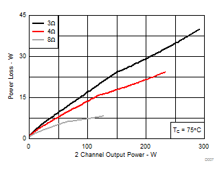
All Measurements taken at audio frequency = 1 kHz, PVDD_X = 30 V, GVDD_X = 12 V, RL = 4 Ω, fS = 600 kHz, ROC = 22 kΩ, TC = 75°C, Output Filter: LDEM = 10 μH, CDEM = 1 µF, mode = 00, AES17 + AUX-0025 measurement filters,unless otherwise noted.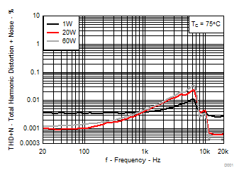
| RL = 4 Ω | P = 1W, 20W, 60W | TC = 75°C |
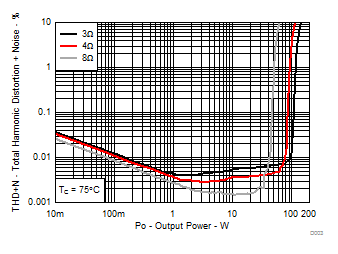
| RL = 3 Ω, 4 Ω, 8 Ω | TC = 75°C |
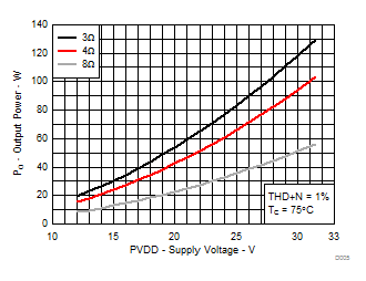
| RL = 3 Ω, 4 Ω, 8 Ω | THD+N = 1% | TC = 75°C |
| RL = 3 Ω, 4 Ω, 8 Ω | THD+N = 10% | TC = 75°C |
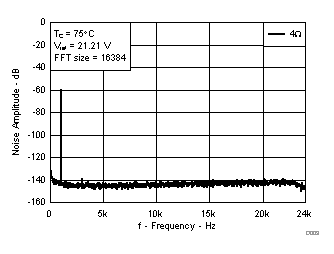
| 4 Ω, VREF = 21.21 V (1% Output power) | FFT = 16384 | |||
| AUX-0025 filter, 80 kHz analyzer BW | TC = 75°C | |||
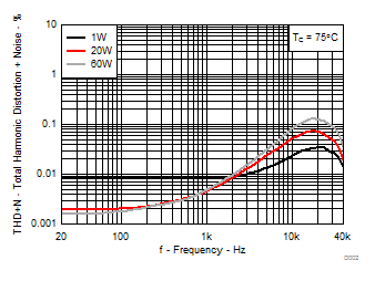
| RL = 4 Ω | P = 1W, 20W, 60W | TC = 75°C |
| AUX-0025 filter, 80 kHz analyzer BW | ||
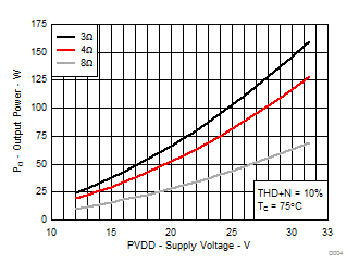
| RL = 3 Ω, 4 Ω, 8 Ω | THD+N = 10% | TC = 75°C |
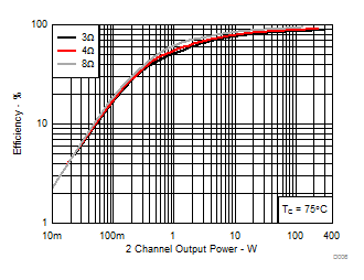
| RL = 3 Ω, 4 Ω, 8 Ω | THD+N = 10% | TC = 75°C |
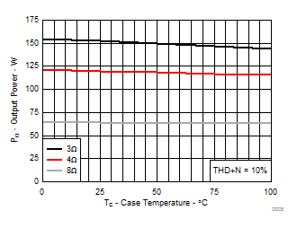
| RL = 3 Ω, 4 Ω, 8 Ω | THD+N = 10% | TC = 75°C |
7.10 Typical Characteristics, SE Configuration
All Measurements taken at audio frequency = 1 kHz, PVDD_X = 30 V, GVDD_X = 12 V, RL = 3 Ω, fS = 600 kHz, ROC = 22 kΩ, TC = 75°C, Output Filter: LDEM = 15 μH, CDEM = 680 nF, MODE = 11, AES17 + AUX-0025 measurement filters, unless otherwise noted.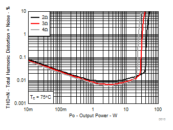
| RL = 2Ω, 3Ω, 4Ω | TC = 75°C |
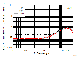
| RL = 3Ω | P = 1W, 5W, 20W | TC = 75°C |
| AUX-0025 filter, 80 kHz analyzer BW | ||
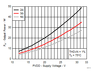
| RL = 2Ω, 3Ω, 4Ω | THD+N = 1% | TC = 75°C |
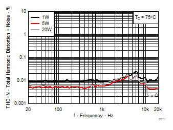
| RL = 3Ω | P = 1W, 5W, 20W | TC = 75°C |
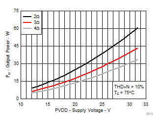
| RL = 2Ω, 3Ω, 4Ω | THD+N = 10% | TC = 75°C |
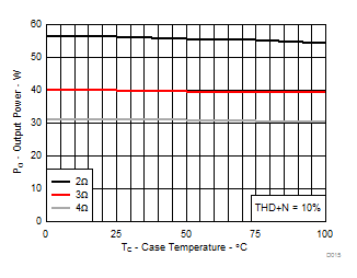
| RL = 2Ω, 3Ω, 4Ω | THD+N = 10% | TC = 75°C |
7.11 Typical Characteristics, PBTL Configuration
All Measurements taken at audio frequency = 1kHz, PVDD_X = 30V, GVDD_X = 12V, RL = 2Ω, fS = 600 kHz, ROC = 22kΩ, TC = 75°C, Output Filter: LDEM = 10μH, CDEM = 1 µF, MODE = 10, outputs paralleled before LC filter, AES17 + AUX-0025 measurement filters, unless otherwise noted.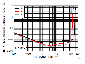
| RL = 2Ω, 3Ω, 4Ω | TC = 75°C |
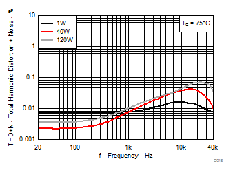
| RL = 2Ω | P = 1W, 40W, 120W | TC = 75°C |
| AUX-0025 filter, 80 kHz analyzer BW | ||
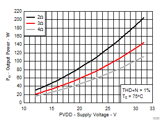
| RL = 2Ω, 3Ω, 4Ω | THD+N = 1% | TC = 75°C |

| RL = 2Ω | P = 1W, 40W, 120W | TC = 75°C |
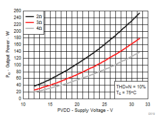
| RL = 2Ω, 3Ω, 4Ω | THD+N = 10% | TC = 75°C |
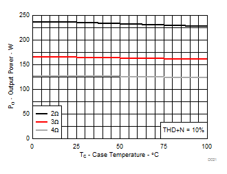
| RL = 2Ω, 3Ω, 4Ω | THD+N = 10% | TC = 75°C |