ZHCSDT9C June 2015 – June 2015
PRODUCTION DATA.
- 1 特性
- 2 应用
- 3 说明
- 4 修订历史记录
- 5 Device Comparison Table
- 6 Pin Configuration and Functions
-
7 Specifications
- 7.1 Absolute Maximum Ratings
- 7.2 ESD Ratings
- 7.3 Recommended Operating Conditions
- 7.4 Thermal Information
- 7.5 Electrical Characteristics
- 7.6 Audio Characteristics (BTL)
- 7.7 Audio Characteristics (SE)
- 7.8 Audio Characteristics (PBTL)
- 7.9 Typical Characteristics, BTL Configuration
- 7.10 Typical Characteristics, SE Configuration
- 7.11 Typical Characteristics, PBTL Configuration
- 8 Parameter Measurement Information
- 9 Detailed Description
- 10Application and Implementation
- 11Power Supply Recommendations
- 12Layout
- 13器件和文档支持
- 14机械、封装和可订购信息
9 Detailed Description
9.1 Overview
To facilitate system design, the TPA3251D2 needs only a 12-V supply in addition to the (typical) 36-V power-stage supply. An internal voltage regulator provides suitable voltage levels for the digital and low-voltage analog circuitry, AVDD and DVDD. Additionally, all circuitry requiring a floating voltage supply, that is, the high-side gate drive, is accommodated by built-in bootstrap circuitry requiring only an external capacitor for each half-bridge.
The audio signal path including gate drive and output stage is designed as identical, independent half-bridges. For this reason, each half-bridge has separate bootstrap pins (BST_X). Power-stage supply pins (PVDD_X) and gate drive supply pins (GVDD_X) are separate for each full bridge. Although supplied from the same 12-V source, separating to GVDD_AB, GVDD_CD, and VDD on the printed-circuit board (PCB) by RC filters (see application diagram for details) is recommended. These RC filters provide the recommended high-frequency isolation. Special attention should be paid to placing all decoupling capacitors as close to their associated pins as possible. In general, the physical loop with the power supply pins, decoupling capacitors and GND return path to the device pins must be kept as short as possible and with as little area as possible to minimize induction (see reference board documentation for additional information).
For a properly functioning bootstrap circuit, a small ceramic capacitor must be connected from each bootstrap pin (BST_X) to the power-stage output pin (OUT_X). When the power-stage output is low, the bootstrap capacitor is charged through an internal diode connected between the gate-drive power-supply pin (GVDD_X) and the bootstrap pins. When the power-stage output is high, the bootstrap capacitor potential is shifted above the output potential and thus provides a suitable voltage supply for the high-side gate driver. It is recommended to use 33-nF ceramic capacitors, size 0603 or 0805, for the bootstrap supply. These 33nF capacitors ensure sufficient energy storage, even during minimal PWM duty cycles, to keep the high-side power stage FET (LDMOS) fully turned on during the remaining part of the PWM cycle.
Special attention should be paid to the power-stage power supply; this includes component selection, PCB placement, and routing. As indicated, each full-bridge has independent power-stage supply pins (PVDD_X). For optimal electrical performance, EMI compliance, and system reliability, it is important that each PVDD_X node is decoupled with 1-μF ceramic capacitor placed as close as possible to the supply pins. It is recommended to follow the PCB layout of the TPA3251D2 reference design. For additional information on recommended power supply and required components, see the application diagrams in this data sheet.
The 12-V supply should be from a low-noise, low-output-impedance voltage regulator. Likewise, the 36-V power-stage supply is assumed to have low output impedance and low noise. The power-supply sequence is not critical as facilitated by the internal power-on-reset circuit, but it is recommended to release RESET after the power supply is settled for minimum turn on audible artefacts. Moreover, the TPA3251D2 is fully protected against erroneous power-stage turn on due to parasitic gate charging. Thus, voltage-supply ramp rates (dV/dt) are non-critical within the specified range (see the Recommended Operating Conditions table of this data sheet).
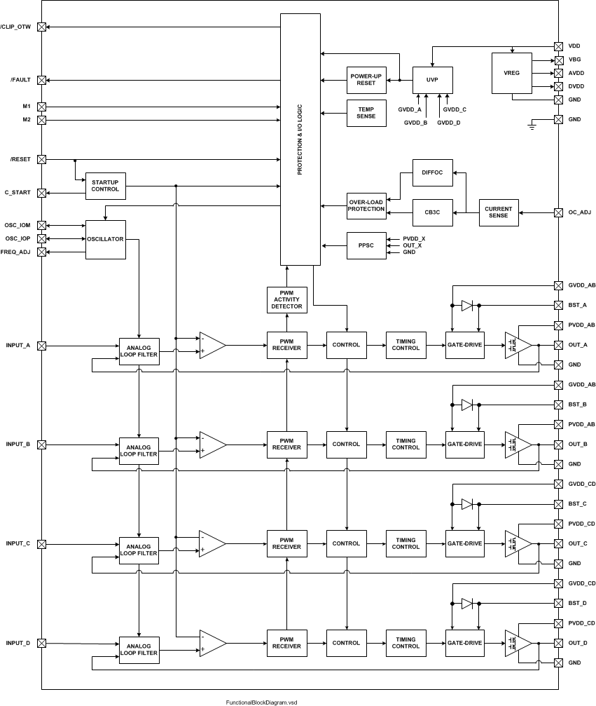
9.2 Functional Block Diagrams

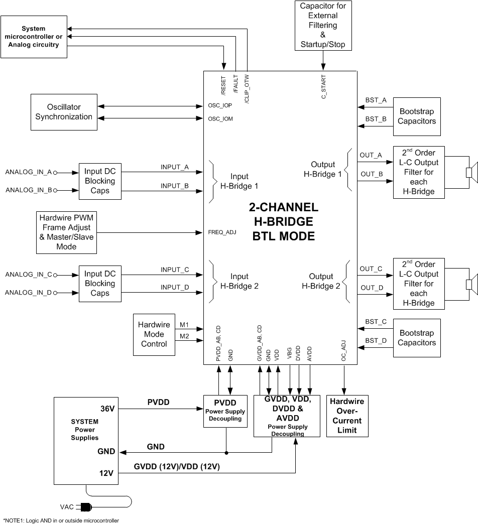
 Figure 22. System Block Diagram
9.3 Feature Description
9.3.1 Error Reporting
The FAULT, and CLIP_OTW, pins are active-low, open-drain outputs. The function is for protection-mode signaling to a system-control device.
Any fault resulting in device shutdown is signaled by the FAULT pin going low. Also, CLIP_OTW goes low when the device junction temperature exceeds 125°C (see Table 2).
Table 2. Error Reporting
| FAULT | CLIP_OTW | DESCRIPTION |
|---|---|---|
| 0 | 0 | Overtemperature (OTE) or overload (OLP) or undervoltage (UVP) Junction temperature higher than 125°C (overtemperature warning) |
| 0 | 0 | Overload (OLP) or undervoltage (UVP). Junction temperature higher than 125°C (overtemperature warning) |
| 0 | 1 | Overload (OLP) or undervoltage (UVP). Junction temperature lower than 125°C |
| 1 | 0 | Junction temperature higher than 125°C (overtemperature warning) |
| 1 | 1 | Junction temperature lower than 125°C and no OLP or UVP faults (normal operation) |
Note that asserting either RESET low forces the FAULT signal high, independent of faults being present. TI recommends monitoring the CLIP_OTW signal using the system microcontroller and responding to an overtemperature warning signal by, that is, turning down the volume to prevent further heating of the device resulting in device shutdown (OTE).
To reduce external component count, an internal pullup resistor to 3.3 V is provided on both FAULT and CLIP_OTW outputs.
9.4 Device Protection System
The TPA3251D2 contains advanced protection circuitry carefully designed to facilitate system integration and ease of use, as well as to safeguard the device from permanent failure due to a wide range of fault conditions such as short circuits, overload, overtemperature, and undervoltage. The TPA3251D2 responds to a fault by immediately setting the power stage in a high-impedance (Hi-Z) state and asserting the FAULT pin low. In situations other than overload and overtemperature error (OTE), the device automatically recovers when the fault condition has been removed, that is, the supply voltage has increased.
The device will function on errors, as shown in Table 3.
Table 3. Device Protection
| BTL | MODE | PBTL | MODE | SE | MODE |
|---|---|---|---|---|---|
| LOCAL ERROR IN | TURNS OFF | LOCAL ERROR IN | TURNS OFF | LOCAL ERROR IN | TURNS OFF |
| A | A+B | A | A+B+C+D | A | A+B |
| B | B | B | |||
| C | C+D | C | C | C+D | |
| D | D | D |
Bootstrap UVP does not shutdown according to the table, it shuts down the respective halfbridge (non-latching, does not assert FAULT).
9.4.1 Overload and Short Circuit Current Protection
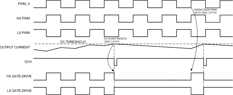
TPA3251D2 has fast reacting current sensors with a programmable trip threshold (OC threshold) on all high-side and low-side FETs. To prevent output current to increase beyond the programmed threshold, TPA3251D2 has the option of either limiting the output current for each switching cycle (Cycle By Cycle Current Control, CB3C) or to perform an immediate shutdown of the output in case of excess output current (Latching Shutdown). CB3C prevents premature shutdown due to high output current transients caused by high level music transients and a drop of real speaker’s load impedance, and allows the output current to be limited to a maximum programmed level. If the maximum output current persists, i.e. the power stage being overloaded with too low load impedance, the device will shut down the affected output channel and the affected output is put in a high-impedance (Hi- Z) state until a RESET cycle is initiated. CB3C works individually for each half bridge output. If an over current event is triggered, CB3C performs a state flip of the half bridge output that is cleared upon beginning of next PWM frame.
 Figure 23. CB3C Timing Example
During CB3C an over load counter increments for each over current event and decrease for each non-over current PWM cycle. This allows full amplitude transients into a low speaker impedance without a shutdown protection action. In the event of a short circuit condition, the over current protection limits the output current by the CB3C operation and eventually shut down the affected output if the overload counter reaches its maximum value. If a latched OC operation is required such that the device shuts down the affected output immediately upon first detected over current event, this protection mode should be selected. The over current threshold and mode (CB3C or Latched OC) is programmed by the OC_ADJ resistor value. The OC_ADJ resistor needs to be within its intentional value range for either CB3C operation or Latched OC operation.
 Figure 24. OC Threshold versus OC_ADJ Resistor Value Example
OC_ADJ values outside specified value range for either CB3C or latched OC operation will result in minimum OC threshold.
Table 4. Device Protection
| OC_ADJ Resistor Value | Protection Mode | OC Threshold |
|---|---|---|
| 22kΩ | CB3C | 16.3A |
| 24kΩ | CB3C | 15.1A |
| 27kΩ | CB3C | 13.5A |
| 30kΩ | CB3C | 12.3A |
| 47kΩ | Latched OC | 16.3A |
| 51kΩ | Latched OC | 15.1A |
| 56kΩ | Latched OC | 13.5A |
| 64kΩ | Latched OC | 12.3A |
9.4.2 DC Speaker Protection
The output DC protection scheme protects a connected speaker from excess DC current caused by a speaker wire accidentally shorted to chassis ground. Such a short circuit results in a DC voltage of PVDD/2 across the speaker, which potentially can result in destructive current levels. The output DC protection detects any unbalance of the output and input current of a BTL output, and in the event of the unbalance exceeding a programmed threshold, the overload counter increments until its maximum value and the affected output channel is shut down. DC Speaker Protection is disabled in PBTL and SE mode operation.
9.4.3 Pin-to-Pin Short Circuit Protection (PPSC)
The PPSC detection system protects the device from permanent damage in the case that a power output pin (OUT_X) is shorted to GND_X or PVDD_X. For comparison, the OC protection system detects an overcurrent after the demodulation filter where PPSC detects shorts directly at the pin before the filter. PPSC detection is performed at startup i.e. when VDD is supplied, consequently a short to either GND_X or PVDD_X after system startup does not activate the PPSC detection system. When PPSC detection is activated by a short on the output, all half bridges are kept in a Hi-Z state until the short is removed; the device then continues the startup sequence and starts switching. The detection is controlled globally by a two step sequence. The first step ensures that there are no shorts from OUT_X to GND_X, the second step tests that there are no shorts from OUT_X to PVDD_X. The total duration of this process is roughly proportional to the capacitance of the output LC filter. The typical duration is < 15ms/μF. While the PPSC detection is in progress, FAULT is kept low, and the device will not react to changes applied to the RESET pin. If no shorts are present the PPSC detection passes, and FAULT is released. A device reset will not start a new PPSC detection. PPSC detection is enabled in BTL and PBTL output configurations, the detection is not performed in SE mode. To make sure not to trip the PPSC detection system it is recommended not to insert a resistive load to GND_X or PVDD_X.
9.4.4 Overtemperature Protection OTW and OTE
TPA3251D2 has a two-level temperature-protection system that asserts an active-low warning signal (CLIP_OTW) when the device junction temperature exceeds 125°C (typical) and, if the device junction temperature exceeds 155°C (typical), the device is put into thermal shutdown, resulting in all half-bridge outputs being set in the high-impedance (Hi-Z) state and FAULT being asserted low. OTE is latched in this case. To clear the OTE latch, RESET must be asserted. Thereafter, the device resumes normal operation.
9.4.5 Undervoltage Protection (UVP) and Power-on Reset (POR)
The UVP and POR circuits of the TPA3251D2 fully protect the device in any power-up/down and brownout situation. While powering up, the POR circuit resets the overload circuit (OLP) and ensures that all circuits are fully operational when the GVDD_X and VDD supply voltages reach stated in the Electrical Characteristics table. Although GVDD_X and VDD are independently monitored, a supply voltage drop below the UVP threshold on any VDD or GVDD_X pin results in all half-bridge outputs immediately being set in the high-impedance (Hi-Z) state and FAULT being asserted low. The device automatically resumes operation when all supply voltages have increased above the UVP threshold.
9.4.6 Fault Handling
If a fault situation occurs while in operation, the device acts accordingly to the fault being a global or a channel fault. A global fault is a chip-wide fault situation and causes all PWM activity of the device to be shut down, and will assert FAULT low. A global fault is a latching fault and clearing FAULT and restart operation requires resetting the device by toggling RESET. Toggling RESET should never be allowed with excessive system temperature, so it is advised to monitor RESET by a system microcontroller and only allow releasing RESET (RESET high) if the OTW signal is cleared (high). A channel fault results in shutdown of the PWM activity of the affected channel(s). Note that asserting RESET low forces the FAULT signal high, independent of faults being present. TI recommends monitoring the OTW signal using the system micro controller and responding to an over temperature warning signal by, that is, turning down the volume to prevent further heating of the device resulting in device shutdown (OTE).
Table 5. Error Reporting
| Fault/Event | Fault/Event Description | Global or Channel | Reporting Method | Latched/Self Clearing | Action needed to Clear | Output FETs |
|---|---|---|---|---|---|---|
| PVDD_X UVP | Voltage Fault | Global | FAULT pin | Self Clearing | Increase affected supply voltage | HI-Z |
| VDD UVP | ||||||
| AVDD UVP | ||||||
| POR (DVDD UVP) | Power On Reset | Global | FAULT pin | Self Clearing | Allow DVDD to rise | HI-Z |
| BST_X UVP | Voltage Fault | Channel (Half Bridge) | None | Self Clearing | Allow BST cap to recharge (lowside ON, VDD 12V) | HighSide off |
| OTW | Thermal Warning | Global | OTW pin | Self Clearing | Cool below OTW threshold | Normal operation |
| OTE | Thermal Shutdown | Global | FAULT pin | Latched | Toggle RESET | HI-Z |
| OLP (CB3C>1.7ms) | OC Shutdown | Channel | FAULT pin | Latched | Toggle RESET | HI-Z |
| Latched OC (47kΩ<ROC_ADJ<68kΩ) | OC Shutdown | Channel | FAULT pin | Latched | Toggle RESET | HI-Z |
| CB3C (22kΩ<ROC_ADJ<30kΩ) | OC Limiting | Channel | None | Self Clearing | Reduce signal level or remove short | Flip state, cycle by cycle at fs/3 |
| Stuck at Fault(1) | No OSC_IO activity in Slave Mode | Global | None | Self Clearing | Resume OSC_IO activity | HI-Z |
9.4.7 Device Reset
Asserting RESET low initiates the device ramp down. The output FETs go into a Hi-Z state after the ramp down is complete. Output pull downs are active both in SE mode and BTL mode with RESET low.
In BTL modes, to accommodate bootstrap charging prior to switching start, asserting the reset input low enables weak pulldown of the half-bridge outputs.
Asserting reset input low removes any fault information to be signaled on the FAULT output, that is, FAULT is forced high. A rising-edge transition on reset input allows the device to resume operation after an overload fault. To ensure thermal reliability, the rising edge of reset must occur no sooner than 4 ms after the falling edge of FAULT.