ZHCSDT9C June 2015 – June 2015
PRODUCTION DATA.
- 1 特性
- 2 应用
- 3 说明
- 4 修订历史记录
- 5 Device Comparison Table
- 6 Pin Configuration and Functions
-
7 Specifications
- 7.1 Absolute Maximum Ratings
- 7.2 ESD Ratings
- 7.3 Recommended Operating Conditions
- 7.4 Thermal Information
- 7.5 Electrical Characteristics
- 7.6 Audio Characteristics (BTL)
- 7.7 Audio Characteristics (SE)
- 7.8 Audio Characteristics (PBTL)
- 7.9 Typical Characteristics, BTL Configuration
- 7.10 Typical Characteristics, SE Configuration
- 7.11 Typical Characteristics, PBTL Configuration
- 8 Parameter Measurement Information
- 9 Detailed Description
- 10Application and Implementation
- 11Power Supply Recommendations
- 12Layout
- 13器件和文档支持
- 14机械、封装和可订购信息
12 Layout
12.1 Layout Guidelines
- Use an unbroken ground plane to have good low impedance and inductance return path to the power supply for power and audio signals.
- Maintain a contiguous ground plane from the ground pins to the PCB area surrounding the device for as many of the ground pins as possible, since the ground pins are the best conductors of heat in the package.
- PCB layout, audio performance and EMI are linked closely together.
- Routing the audio input should be kept short and together with the accompanied audio source ground.
- The small bypass capacitors on the PVDD lines of the DUT be placed as close the PVDD pins as possible.
- A local ground area underneath the device is important to keep solid to minimize ground bounce.
- Orient the passive component so that the narrow end of the passive component is facing the TPA3251D2 device, unless the area between two pads of a passive component is large enough to allow copper to flow in between the two pads.
- Avoid placing other heat producing components or structures near the TPA3251D2 device.
- Avoid cutting off the flow of heat from the TPA3251D2 device to the surrounding ground areas with traces or via strings, especially on output side of device.
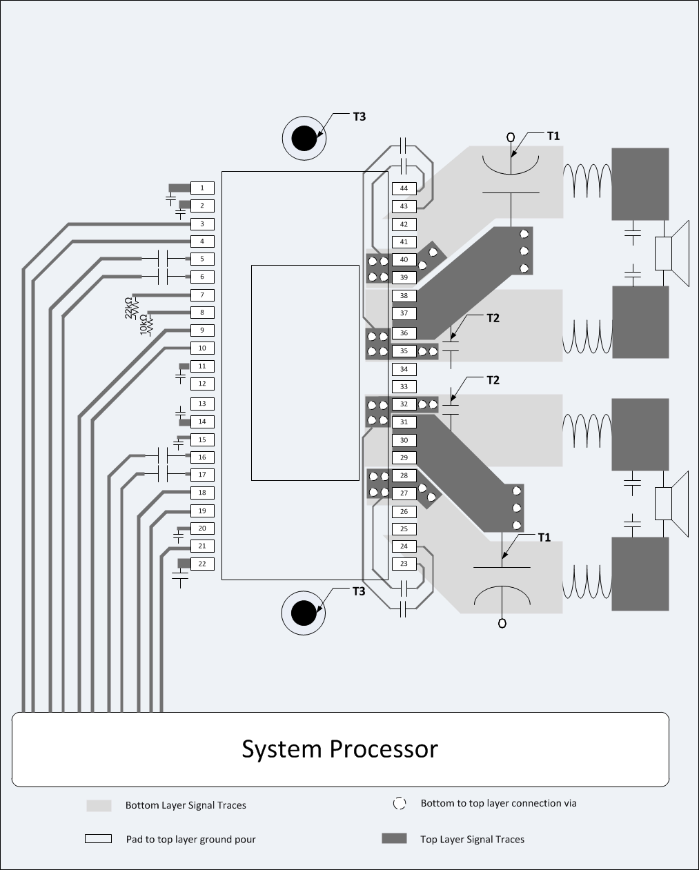
Netlist for this printed circuit board is generated from the schematic in Figure 29.
12.2 Layout Examples
12.2.1 BTL Application Printed Circuit Board Layout Example

A. Note: PCB layout example shows composite layout. Dark grey: Top layer copper traces, light gray: Bottom layer copper traces. All PCB area not used for traces should be GND copper pour (transparent on example image)
B. Note T1: PVDD decoupling bulk capacitors should be as close as possible to the PVDD and GND_X pins, the heat sink sets the distance. Wide traces should be routed on the top layer with direct connection to the pins and without going through vias. No vias or traces should be blocking the current path.
C. Note T2: Close decoupling of PVDD with low impedance X7R ceramic capacitors is placed under the heat sink and close to the pins.
D. Note T3: Heat sink needs to have a good connection to PCB ground.
Figure 29. BTL Application Printed Circuit Board - Composite
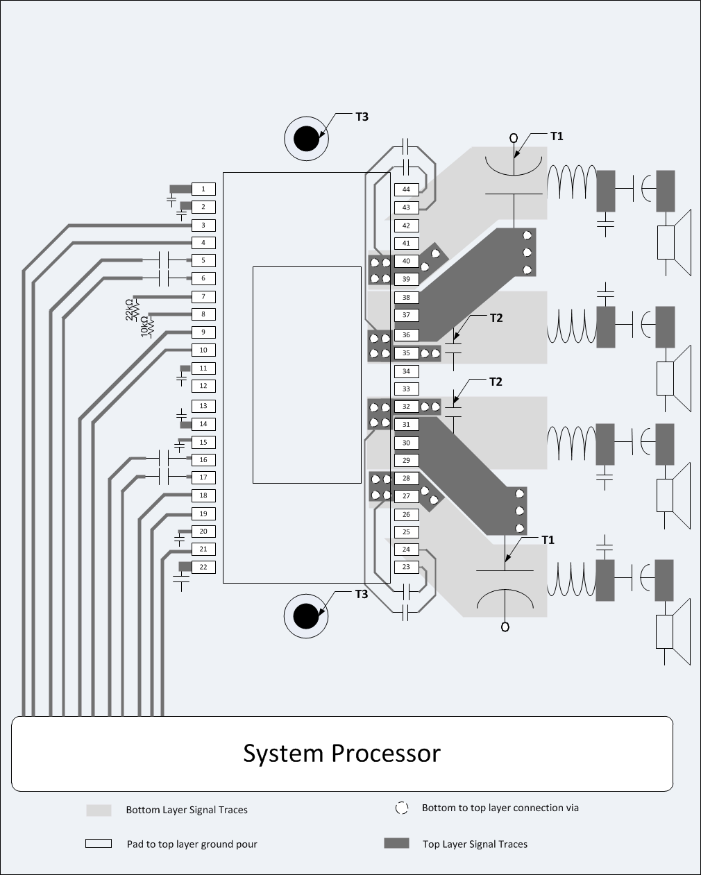
12.2.2 SE Application Printed Circuit Board Layout Example

A. Note: PCB layout example shows composite layout. Dark grey: Top layer copper traces, light gray: Bottom layer copper traces. All PCB area not used for traces should be GND copper pour (transparent on example image)
B. Note T1: PVDD decoupling bulk capacitors should be as close as possible to the PVDD and GND_X pins, the heat sink sets the distance. Wide traces should be routed on the top layer with direct connection to the pins and without going through vias. No vias or traces should be blocking the current path.
C. Note T2: Close decoupling of PVDD with low impedance X7R ceramic capacitors is placed under the heat sink and close to the pins.
D. Note T3: Heat sink needs to have a good connection to PCB ground.
Figure 30. SE Application Printed Circuit Board - Composite
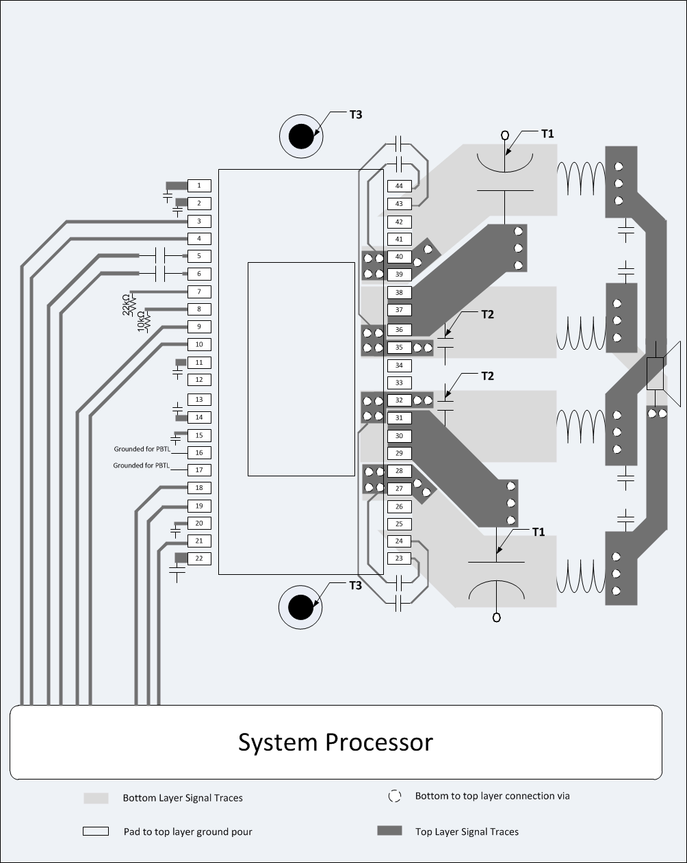
12.2.3 PBTL Application Printed Circuit Board Layout Example

A. Note: PCB layout example shows composite layout. Dark grey: Top layer copper traces, light gray: Bottom layer copper traces. All PCB area not used for traces should be GND copper pour (transparent on example image)
B. Note T1: PVDD decoupling bulk capacitors should be as close as possible to the PVDD and GND_X pins, the heat sink sets the distance. Wide traces should be routed on the top layer with direct connection to the pins and without going through vias. No vias or traces should be blocking the current path.
C. Note T2: Close decoupling of PVDD with low impedance X7R ceramic capacitors is placed under the heat sink and close to the pins.
D. ote T3: Heat sink needs to have a good connection to PCB ground.
Figure 31. PBTL Application Printed Circuit Board - Composite