ZHCSDT9C June 2015 – June 2015
PRODUCTION DATA.
- 1 特性
- 2 应用
- 3 说明
- 4 修订历史记录
- 5 Device Comparison Table
- 6 Pin Configuration and Functions
-
7 Specifications
- 7.1 Absolute Maximum Ratings
- 7.2 ESD Ratings
- 7.3 Recommended Operating Conditions
- 7.4 Thermal Information
- 7.5 Electrical Characteristics
- 7.6 Audio Characteristics (BTL)
- 7.7 Audio Characteristics (SE)
- 7.8 Audio Characteristics (PBTL)
- 7.9 Typical Characteristics, BTL Configuration
- 7.10 Typical Characteristics, SE Configuration
- 7.11 Typical Characteristics, PBTL Configuration
- 8 Parameter Measurement Information
- 9 Detailed Description
- 10Application and Implementation
- 11Power Supply Recommendations
- 12Layout
- 13器件和文档支持
- 14机械、封装和可订购信息
6 Pin Configuration and Functions
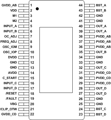
The TPA3251D2 is available in a thermally enhanced TSSOP package.
The package type contains a heat slug that is located on the top side of the device for convenient thermal coupling to the heat sink.
DDV Package
HTSSOP 44-Pin
(Top View)

Pin Functions
| NAME | NO. | I/O | DESCRIPTION |
|---|---|---|---|
| AVDD | 14 | P | Internal voltage regulator, analog section |
| BST_A | 44 | P | HS bootstrap supply (BST), external 0.033 μF capacitor to OUT_A required. |
| BST_B | 43 | P | HS bootstrap supply (BST), external 0.033 μF capacitor to OUT_B required. |
| BST_C | 24 | P | HS bootstrap supply (BST), external 0.033 μF capacitor to OUT_C required. |
| BST_D | 23 | P | HS bootstrap supply (BST), external 0.033 μF capacitor to OUT_D required. |
| CLIP_OTW | 21 | O | Clipping warning and Over-temperature warning; open drain; active low |
| C_START | 15 | O | Startup ramp, requires a charging capacitor to GND |
| DVDD | 11 | P | Internal voltage regulator, digital section |
| FAULT | 19 | O | Shutdown signal, open drain; active low |
| FREQ_ADJ | 8 | O | Oscillator freqency programming pin |
| GND | 12, 13, 25, 26, 33, 34, 41, 42 | P | Ground |
| GVDD_AB | 1 | P | Gate-drive voltage supply; AB-side, requires 0.1 µF capacitor to GND |
| GVDD_CD | 22 | P | Gate-drive voltage supply; CD-side, requires 0.1 µF capacitor to GND |
| INPUT_A | 5 | I | Input signal for half bridge A |
| INPUT_B | 6 | I | Input signal for half bridge B |
| INPUT_C | 16 | I | Input signal for half bridge C |
| INPUT_D | 17 | I | Input signal for half bridge D |
| M1 | 3 | I | Mode selection 1 (LSB) |
| M2 | 4 | I | Mode selection 2 (MSB) |
| OC_ADJ | 7 | I/O | Over-Current threshold programming pin |
| OSC_IOM | 9 | I/O | Oscillator synchronization interface |
| OSC_IOP | 10 | O | Oscillator synchronization interface |
| OUT_A | 39, 40 | O | Output, half bridge A |
| OUT_B | 35 | O | Output, half bridge B |
| OUT_C | 32 | O | Output, half bridge C |
| OUT_D | 27, 28 | O | Output, half bridge D |
| PVDD_AB | 36, 37, 38 | P | PVDD supply for half-bridge A and B |
| PVDD_CD | 29, 30, 31 | P | PVDD supply for half-bridge C and D |
| RESET | 18 | I | Device reset Input; active low |
| VDD | 2 | P | Power supply for internal voltage regulator requires a 10-µF capacitor with a 0.1-µF capacitor to GND for decoupling. |
| VBG | 20 | P | Internal voltage reference requires a 0.1-µF capacitor to GND for decoupling. |
| PowerPad™ | P | Ground, connect to grounded heat sink |
Table 1. Mode Selection Pins
| MODE PINS | INPUT MODE | OUTPUT CONFIGURATION | DESCRIPTION | |||
|---|---|---|---|---|---|---|
| M2 | M1 | |||||
| 0 | 0 | 2N + 1 | 2 × BTL | Stereo BTL output configuration | ||
| 0 | 1 | 2N/1N + 1 | 1 x BTL + 2 x SE | 2.1 BTL + SE mode | ||
| 1 | 0 | 2N + 1 | 1 x PBTL | Parallelled BTL configuration. Connect INPUT_C and INPUT_D to GND. | ||
| 1 | 1 | 1N +1 | 4 x SE | Single ended output configuration | ||