ZHCSJA2A January 2019 – March 2019 TPA3255-Q1
PRODUCTION DATA.
- 1 特性
- 2 应用
- 3 说明
- 4 修订历史记录
- 5 Pin Configuration and Functions
-
6 Specifications
- 6.1 Absolute Maximum Ratings
- 6.2 ESD Ratings
- 6.3 Recommended Operating Conditions
- 6.4 Thermal Information
- 6.5 Electrical Characteristics
- 6.6 Audio Characteristics (BTL)
- 6.7 Audio Characteristics (SE)
- 6.8 Audio Characteristics (PBTL)
- 6.9 Typical Characteristics, BTL Configuration
- 6.10 Typical Characteristics, SE Configuration
- 6.11 Typical Characteristics, PBTL Configuration
- 7 Parameter Measurement Information
-
8 Detailed Description
- 8.1 Overview
- 8.2 Functional Block Diagrams
- 8.3 Feature Description
- 8.4
Device Functional Modes
- 8.4.1
Device Protection System
- 8.4.1.1 Overload and Short Circuit Current Protection
- 8.4.1.2 Signal Clipping and Pulse Injector
- 8.4.1.3 DC Speaker Protection
- 8.4.1.4 Pin-to-Pin Short Circuit Protection (PPSC)
- 8.4.1.5 Overtemperature Protection OTW and OTE
- 8.4.1.6 Undervoltage Protection (UVP) and Power-on Reset (POR)
- 8.4.1.7 Fault Handling
- 8.4.1.8 Device Reset
- 8.4.1
Device Protection System
- 9 Application and Implementation
- 10Power Supply Recommendations
- 11Layout
- 12器件和文档支持
- 13机械、封装和可订购信息
6.9 Typical Characteristics, BTL Configuration
All Measurements taken at audio frequency = 1 kHz, PVDD_X = 51 V, GVDD_X = 10.6 V, RL = 4 Ω, fS = 450 kHz, ROC = 22 kΩ, TC = 75°C, Output Filter: LDEM = 10 μH, CDEM = 1 µF, mode = 00, AES17 + AUX-0025 measurement filters,unless otherwise noted.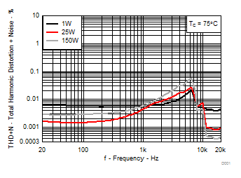
| RL = 4 Ω | P = 1W, 25W, 150W | TC = 75°C |
| PVDD = 51V |
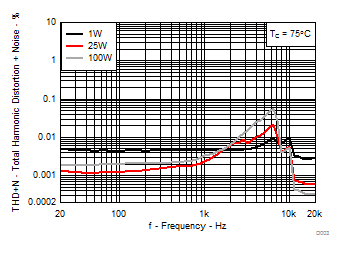
A.
Figure 3. Total Harmonic Distortion+Noise vs Frequency | RL = 8 Ω | P = 1W, 25W, 100W | TC = 75°C |
| PVDD = 53.5V |
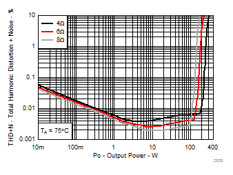
| RL = 4 Ω, 6 Ω, 8 Ω | TC = 75°C | PVDD = 51V |
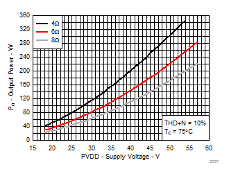
| RL = 4 Ω, 6 Ω, 8 Ω | THD+N = 10% | TC = 75°C |
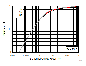
| RL = 4 Ω, 6 Ω, 8 Ω | THD+N = 10% | TC = 75°C |
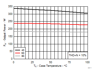
| RL = 4 Ω, 6 Ω, 8 Ω | THD+N = 10% | TC = 75°C |
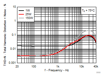
| RL = 4 Ω | P = 1W, 25W, 150W | TC = 75°C |
| AUX-0025 filter, 80 kHz analyzer BW | PVDD = 51V | |
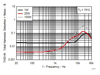
A.
Figure 4. Total Harmonic Distortion+Noise vs Frequency | RL = 8 Ω | P = 1W, 25W, 100W | TC = 75°C |
| AUX-0025 filter, 80 kHz analyzer BW | PVDD = 53.5V | |
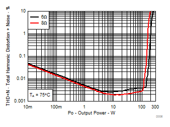
A.
Figure 6. Total Harmonic Distortion + Noise vs Output Power | RL = 6 Ω, 8 Ω | TC = 75°C | PVDD = 53.5V |
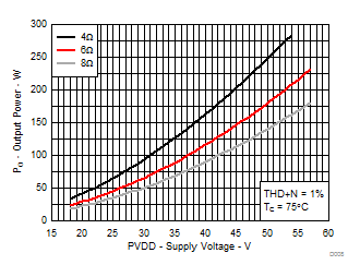
| RL = 4 Ω, 6 Ω, 8 Ω | THD+N = 1% | TC = 75°C |
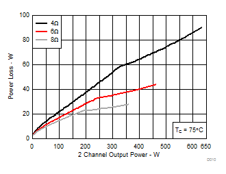
| RL = 4 Ω, 6 Ω, 8 Ω | THD+N = 10% | TC = 75°C |
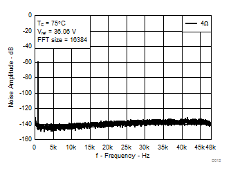
| 4 Ω, VREF = 36.06 V (1% Output power) | FFT = 16384 | |||
| AUX-0025 filter, 80 kHz analyzer BW | TC = 75°C | |||