ZHCSJA2A January 2019 – March 2019 TPA3255-Q1
PRODUCTION DATA.
- 1 特性
- 2 应用
- 3 说明
- 4 修订历史记录
- 5 Pin Configuration and Functions
-
6 Specifications
- 6.1 Absolute Maximum Ratings
- 6.2 ESD Ratings
- 6.3 Recommended Operating Conditions
- 6.4 Thermal Information
- 6.5 Electrical Characteristics
- 6.6 Audio Characteristics (BTL)
- 6.7 Audio Characteristics (SE)
- 6.8 Audio Characteristics (PBTL)
- 6.9 Typical Characteristics, BTL Configuration
- 6.10 Typical Characteristics, SE Configuration
- 6.11 Typical Characteristics, PBTL Configuration
- 7 Parameter Measurement Information
-
8 Detailed Description
- 8.1 Overview
- 8.2 Functional Block Diagrams
- 8.3 Feature Description
- 8.4
Device Functional Modes
- 8.4.1
Device Protection System
- 8.4.1.1 Overload and Short Circuit Current Protection
- 8.4.1.2 Signal Clipping and Pulse Injector
- 8.4.1.3 DC Speaker Protection
- 8.4.1.4 Pin-to-Pin Short Circuit Protection (PPSC)
- 8.4.1.5 Overtemperature Protection OTW and OTE
- 8.4.1.6 Undervoltage Protection (UVP) and Power-on Reset (POR)
- 8.4.1.7 Fault Handling
- 8.4.1.8 Device Reset
- 8.4.1
Device Protection System
- 9 Application and Implementation
- 10Power Supply Recommendations
- 11Layout
- 12器件和文档支持
- 13机械、封装和可订购信息
10.4.3 Thermal Performance with Non-Continuous Output Power
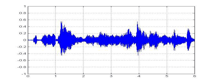
As audio signals often have a peak to average ratio larger than one (average level below maximum peak output), the thermal performance for audio signals can be illustrated using burst signals with different burst ratios.
 Figure 34. Example of audio signal
 A burst signal is characterized by the high-level to low-level ratio as well as the duration of the high level and low level, e.g. a burst 1:4 stimuli is a single period of high level followed by 4 cycles of low level.
 Figure 35. Example of 1:4 Burst Signal
 The following analysis of thermal performance for TPA3255-Q1 is made with the heatsink temperature controlled to 75°C.
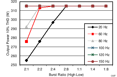
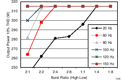
The device is not thermally limited with 8-Ω load, but depending on the burst stimuli for operation at 75ºC heatsink temperature some thermal limitations may occur with a lower load impedance, depending on switching frequency and average to maximum power ratio. The figure below shows burst performance with a signal power ratio of 1:16 (low cycles power level 1/16 of the high cycles power level) and 1:8 .
 Figure 36. Maximum Burst Output Power vs Frequency, BTL, 4Ω Load, Each Channel, TC = 75°C, Power Ratio 1:16
  Figure 37. Maximum Burst Output Power vs Frequency, BTL, 4Ω Load, Each Channel, TC = 75°C, Power Ratio 1:8