ZHCSMX0B September   2019  – December 2020 TPA6304-Q1

PRODUCTION DATA  

  1. 特性
  2. 应用
  3. 说明
  4. Revision History
  5. Pin Configuration and Functions
  6. Specifications
    1. 6.1 Absolute Maximum Ratings
    2. 6.2 ESD Ratings
    3. 6.3 Recommended Operating Conditions
    4. 6.4 Thermal Information
    5. 6.5 Electrical Characteristics
    6. 6.6 Typical Characteristics
      1. 6.6.1 Bridge-Tied Load (BTL), BD
      2. 6.6.2 Parallel Bridge-Tied Load (PBTL)
      3. 6.6.3 Bridge-Tied Load (BTL), 1SPW
      4. 6.6.4 Bridge-Tied Load (BTL), 384 kHz, BD
      5. 6.6.5 Bridge-Tied Load (BTL), 384 kHz, 1SPW
  7. Parameter measurement information
  8. Detailed Description
    1. 7.1 Overview
    2. 7.2 Functional Block Diagram
    3. 7.3 Feature Description
      1. 7.3.1  Single-Ended Analog Inputs
      2. 7.3.2  Gain Control
      3. 7.3.3  Class-D Operation and Spread Spectrum Control
        1. 7.3.3.1 High Frequency Pulse Width Modulator (PWM)
        2. 7.3.3.2 Clock Synchronization
        3. 7.3.3.3 Spread Spectrum Control
      4. 7.3.4  Gate Drive
      5. 7.3.5  Power FETs
      6. 7.3.6  Load Diagnostics
        1. 7.3.6.1 DC Load Diagnostics
          1. 7.3.6.1.1 Automatic DC Load Diagnostics at Device Initialization
          2. 7.3.6.1.2 Automatic DC Load Diagnostics During Hi-Z to MUTE or PLAY Transition
          3. 7.3.6.1.3 Manual Start of DC Load Diagnostics
          4. 7.3.6.1.4 Short-to-Ground
          5. 7.3.6.1.5 Short-to-Power
          6. 7.3.6.1.6 Shorted Load and Open Load
          7. 7.3.6.1.7 Line Output Diagnostics
        2. 7.3.6.2 AC Load Diagnostics
          1. 7.3.6.2.1 Operating Principal
          2. 7.3.6.2.2 Stimulus
          3. 7.3.6.2.3 Load Impedance
          4. 7.3.6.2.4 Tweeter Detection
          5. 7.3.6.2.5 Operation
      7. 7.3.7  Power Supply
        1. 7.3.7.1 Power-Supply Sequence
          1. 7.3.7.1.1 Power-Up Sequence
          2. 7.3.7.1.2 Power-Down Sequence
      8. 7.3.8  Device Initialization and Power-On-Reset (POR)
      9. 7.3.9  Protection and Monitoring
        1. 7.3.9.1 Over Current Protection
        2. 7.3.9.2 DC Detect
        3. 7.3.9.3 Load Current Limit
        4. 7.3.9.4 Clip Detect
        5. 7.3.9.5 Temperature Protection and Monitoring
          1. 7.3.9.5.1 Over Temperature Shutdown (OTSD)
          2. 7.3.9.5.2 Over Temperature Warning (OTW)
          3. 7.3.9.5.3 Thermal Gain Foldback (TGFB)
        6. 7.3.9.6 Power Failures
        7. 7.3.9.7 Load Dump Protection
      10. 7.3.10 Hardware Control Pins
        1. 7.3.10.1 FAULT Pin
        2. 7.3.10.2 STANDBY Pin
        3. 7.3.10.3 GPIO Pins
        4. 7.3.10.4 WARNING
        5. 7.3.10.5 MUTE
    4. 7.4 Device Functional Modes
      1. 7.4.1 Internal Reporting Signals
        1. 7.4.1.1 Fault Signal
        2. 7.4.1.2 Warning Signal
        3. 7.4.1.3 Clip Detect Signal
      2. 7.4.2 Device States and Flags
        1. 7.4.2.1 Audio Channel States
          1. 7.4.2.1.1 PROTECTIVE SHUTDOWN with AUTO RECOVERY State
          2. 7.4.2.1.2 PROTECTIVE SHUTDOWN State
            1. 7.4.2.1.2.1 Clear Fault
        2. 7.4.2.2 Status and Memory Registers
          1. 7.4.2.2.1 Status Registers
          2. 7.4.2.2.2 Memory Registers
      3. 7.4.3 Fault Events
        1. 7.4.3.1 Overview
        2. 7.4.3.2 Power Fault Events
          1. 7.4.3.2.1 DVDD POR
          2. 7.4.3.2.2 VBAT Over Voltage Fault
          3. 7.4.3.2.3 VBAT Under Voltage Fault
          4. 7.4.3.2.4 PVDD Over Voltage Fault
          5. 7.4.3.2.5 PVDD Under Voltage Fault
          6. 7.4.3.2.6 GVDD Fault
        3. 7.4.3.3 Over Temperature Shut Down (OTSD) Event
        4. 7.4.3.4 Over Current Shut Down (OCSD) Event
        5. 7.4.3.5 DC Fault Event
        6. 7.4.3.6 Load Current Fault Event
        7. 7.4.3.7 Invalid Clock Fault Event
      4. 7.4.4 Warning Events
        1. 7.4.4.1 Overview
        2. 7.4.4.2 Over Temperature Warning Event
        3. 7.4.4.3 Thermal Gain Foldback Warning Event
        4. 7.4.4.4 Load Current Warning Event
        5. 7.4.4.5 Clip Warning Event
    5. 7.5 Programming
      1. 7.5.1 I2C Serial Communication Bus
        1. 7.5.1.1 I2C Address Selection
      2. 7.5.2 I2C Bus Protocol
        1. 7.5.2.1 Random Write
        2. 7.5.2.2 Sequential Write
        3. 7.5.2.3 Random Read
        4. 7.5.2.4 Sequential Read
    6. 7.6 Register Maps
      1. 7.6.1 Registers
  9. Application Information Disclaimer
    1. 8.1 Application Information
      1. 8.1.1 AM Radio Avoidance
      2. 8.1.2 Parallel BTL Operation (PBTL)
      3. 8.1.3 Reconstruction Filter Design
      4. 8.1.4 Bootstrap Capacitors
      5. 8.1.5 Line Driver Applications
    2. 8.2 Typical Applications
      1. 8.2.1 BTL Application
        1. 8.2.1.1 Design Requirements
        2. 8.2.1.2 Detailed Hardware Design Procedure
      2. 8.2.2 PBTL Application
        1. 8.2.2.1 Detailed Hardware Design Procedure
  10. Power Supply Recommendations
  11. 10Layout
    1. 10.1 Layout Guidelines
      1. 10.1.1 Electrical Connection of Thermal Pad and Heat Sink
      2. 10.1.2 General Considerations
    2. 10.2 Layout Example
    3. 10.3 Thermal Considerations
  12. 11Device and Documentation Support
    1. 11.1 Documentation Support
      1. 11.1.1 Related Documentation
    2. 11.2 接收文档更新通知
    3. 11.3 支持资源
    4. 11.4 Trademarks
    5. 11.5 静电放电警告
    6. 11.6 术语表

封装选项

机械数据 (封装 | 引脚)
散热焊盘机械数据 (封装 | 引脚)
订购信息
Thermal Gain Foldback (TGFB)

The TGFB circuitry is designed to protect the TPA6304-Q1 from reaching excessive die temperatures. By default, the TGFB is enabled and the device automatically reduces the gain and thereby output power when either the global Over Temperature Warning Event (OTW) or any channel Over Temperature Warning Event, OTW(i) is active. Simultaneously on all channels, the gain is stepped down in 0.5 dB steps with a max attenuation of 12 dB. The gain increases as the temperature is reduced by the same gain step. The attack and release time of the TGFB can be programmed.

The Thermal Gain Foldback Control Register controls whether TGFB is enabled, the rate of gain reduction (attack) and the rate of gain increase or recovery (release). Pop free gain changes are controlled by enabling a zero crossing detector. The zero crossing has a wait time before the gain can change. By default, TGFB and zero crossing detector are enabled with a wait time of 20 µs. Zero Crossing behavior can be adjusted in the Thermal Gain Foldback Control Register. When Thermal Gain Foldback is engaged, that is when the gain is lower than 0 dB a Thermal Gain Foldback Warning Event is created.
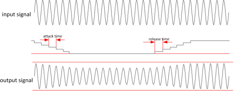
GUID-61F7CD3B-36AB-4FD6-8B20-28E3EC0D2D34-low.gifFigure 7-6 Thermal Foldback Attack and Release