TC = 25°C, PVDD = VBAT =
14.4 V, DVDD = 3.3 V, RL = 4 Ω, Pout = 1 W/ch, ƒOUT
= 1 kHz, FSW = 2.1 MHz, Gain = 22 dB, BD Mode, AES17
Filter, default I2C settings, LC reconstruction filter: 3.3 μH -
ASWPA4035S3R3MT in 4Ω, ASWPA6055S3R3MT in 2 Ω configuration and 1 μF (unless
otherwise noted). See application diagram in Figure 8-2
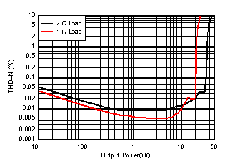
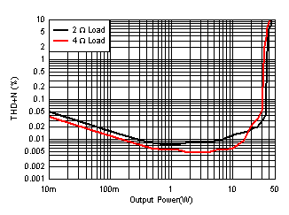
 Figure 6-1 THD+N
vs Power - 2 Ω, 4 Ω - 14.4 V
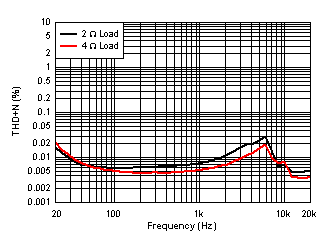
 Figure 6-3 THD+N
vs Frequency - 2 Ω, 4 Ω
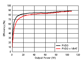
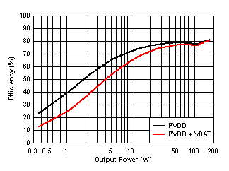
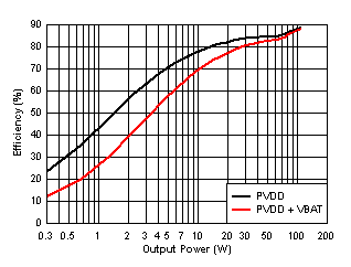
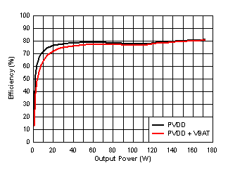
 Figure 6-5 Efficiency vs Output Power - 4 Ω
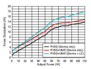
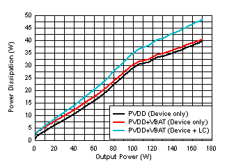
 Figure 6-7 Power
Dissipation vs Output Power - 4 Ω
 Figure 6-9 Efficiency vs Output Power - 2 Ω (Zoomed)
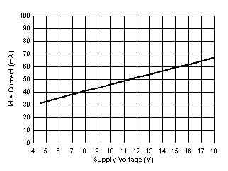
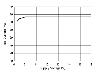
 Figure 6-11 PVDD
Idle vs Supply Voltage
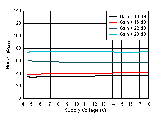
 Figure 6-13 Noise
vs Supply Voltage
| PO = 1 W |
PVDD = 14.4 V + 1 V
RMS |
BTL |
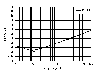
Figure 6-15 PSRR
vs Frequency - PVDD Only
| PO = 1 W |
PVDD = VBAT = 14.4 V + 1 V
RMS |
BTL |
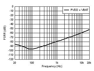
Figure 6-17 PSRR
vs Frequency - PVDD+VBAT Figure 6-2 THD+N
vs Power - 2 Ω, 4 Ω - 18 V
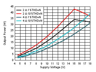
 Figure 6-4 Output Power vs Supply Voltage - 2 Ω 1%, 2 Ω 10%, 4 Ω 1%, 4 Ω 10%
 Figure 6-6 Efficiency vs Output Power - 4 Ω (Zoomed)
 Figure 6-8 Efficiency vs Output Power - 2 Ω
 Figure 6-10 Power
Dissipation vs Output Power - 2 Ω
 Figure 6-12 VBAT
Idle Current vs Supply Voltage
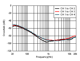
 Figure 6-14 Crosstalk vs Frequency
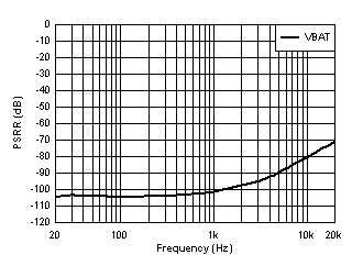
| PO = 1 W |
VBAT = 14.4 V + 1 V
RMS |
BTL |
Figure 6-16 PSRR
vs Frequency - VBAT Only
