ZHCS404F September 2011 – October 2015 TPD12S016
PRODUCTION DATA.
- 1 特性
- 2 应用范围
- 3 说明
- 4 修订历史记录
- 5 Pin Configuration and Functions
- 6 Specifications
-
7 Detailed Description
- 7.1 Overview
- 7.2 Functional Block Diagram
- 7.3
Feature Description
- 7.3.1 Conforms to HDMI Compliance Tests Without any External Components
- 7.3.2 IEC 61000-4-2 ESD Protection
- 7.3.3 Supports HDMI 1.4 Data Rate
- 7.3.4 Matches Class D and Class C Pin Mapping
- 7.3.5 8-Channel ESD Lines for Four Differential Pairs with Ultra-low Differential Capacitance Matching (0.05 pF)
- 7.3.6 On-Chip Load Switch With 55-mA Current Limit Feature at the HDMI 5V_OUT Pin
- 7.3.7 Auto-direction Sensing I2C Level Shifter With One-Shot Circuit to Drive a Long HDMI Cable (750-pF Load)
- 7.3.8 Back-Drive Protection on HDMI Connector Side Ports
- 7.3.9 Integrated Pullup and Pulldown Resistors per HDMI Specification
- 7.3.10 Space Saving 24-Pin RKT Package and 24-TSSOP Package
- 7.3.11 DDC/CEC LEVEL SHIFT Circuit Operation
- 7.3.12 DDC/CEC Level Shifter Operational Notes For VCCA = 1.8 V
- 7.3.13 Rise-Time Accelerators
- 7.3.14 Noise Considerations
- 7.3.15 Resistor Pullup Value Selection
- 7.4 Device Functional Modes
- 8 Application and Implementation
- 9 Power Supply Recommendations
- 10Layout
- 11器件和文档支持
- 12机械、封装和可订购信息
封装选项
请参考 PDF 数据表获取器件具体的封装图。
机械数据 (封装 | 引脚)
- RKT|24
- PW|24
散热焊盘机械数据 (封装 | 引脚)
- RKT|24
订购信息
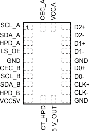
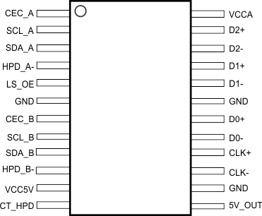
5 Pin Configuration and Functions
RKT Package
24-Pin UQFN
Top View

PW Package
24-Pin TSSOP
Top View

Pin Functions
| PIN | TYPE | DESCRIPTION | ||
|---|---|---|---|---|
| NAME | RKT | PW | ||
| D–, D+ | 16, 17, 19 to 22 | 17, 18, 20 to 23 | IO | HDMI TMDS data. Connect to HDMI controller and HDMI connector directly |
| CLK+, CLK– | 14, 15 | 15, 16 | IO | HDMI TMDS clock. Connect to HDMI controller and HDMI connector directly |
| HPD_A | 3 | 4 | O | Hot plug detect output referenced to VCCA. Connect to HDMI controller hot plug detect input pin |
| HPD_B | 9 | 10 | I | Hot plug detect input. Connect directly to HDMI connector hot plug detect pin |
| CEC_A | 24 | 1 | IO | HDMI controller side CEC signal pin referenced to VCCA. Connect to HDMI controller |
| CEC_B | 6 | 7 | IO | HDMI connector side CEC signal pin referenced to internal 3.3-V supply. Connect to HDMI connector CEC pin |
| SCL_A | 1 | 2 | IO | HDMI controller side SCL signal pin referenced to VCCA. Connect to HDMI controller |
| SCL_B | 7 | 8 | IO | HDMI connector side SCL signal pin referenced to 5V_OUT supply. Connect to HDMI connector SCL pin |
| SDA_A | 2 | 3 | IO | HDMI controller side SDA signal pin referenced to VCCA. Connect to HDMI controller |
| SDA_B | 8 | 9 | IO | HDMI connector side SDA signal pin referenced to 5V_OUT supply. Connect to HDMI connector SDA pin |
| LS_OE | 4 | 5 | I | Disables the Level shifters when OE = L. The OE pin is referenced to VCCA |
| CT_HPD | 11 | 12 | I | Disables the load switch and HPD_B when CT_HPD = L. The CT_HPD is referenced to VCCA |
| VCC5V | 10 | 11 | PWR | Internal 5-V supply (input to the load switch) |
| VCCA | 23 | 24 | PWR | Internal PCB low voltage supply (same as the HDMI controller chip supply) |
| 5V_OUT | 12 | 13 | O | External 5-V supply (output of the load switch) |
| GND | 5, 13, 18 | 6, 14, 19 | GND | Connect to system ground plane |