ZHCS404F September 2011 – October 2015 TPD12S016
PRODUCTION DATA.
- 1 特性
- 2 应用范围
- 3 说明
- 4 修订历史记录
- 5 Pin Configuration and Functions
- 6 Specifications
-
7 Detailed Description
- 7.1 Overview
- 7.2 Functional Block Diagram
- 7.3
Feature Description
- 7.3.1 Conforms to HDMI Compliance Tests Without any External Components
- 7.3.2 IEC 61000-4-2 ESD Protection
- 7.3.3 Supports HDMI 1.4 Data Rate
- 7.3.4 Matches Class D and Class C Pin Mapping
- 7.3.5 8-Channel ESD Lines for Four Differential Pairs with Ultra-low Differential Capacitance Matching (0.05 pF)
- 7.3.6 On-Chip Load Switch With 55-mA Current Limit Feature at the HDMI 5V_OUT Pin
- 7.3.7 Auto-direction Sensing I2C Level Shifter With One-Shot Circuit to Drive a Long HDMI Cable (750-pF Load)
- 7.3.8 Back-Drive Protection on HDMI Connector Side Ports
- 7.3.9 Integrated Pullup and Pulldown Resistors per HDMI Specification
- 7.3.10 Space Saving 24-Pin RKT Package and 24-TSSOP Package
- 7.3.11 DDC/CEC LEVEL SHIFT Circuit Operation
- 7.3.12 DDC/CEC Level Shifter Operational Notes For VCCA = 1.8 V
- 7.3.13 Rise-Time Accelerators
- 7.3.14 Noise Considerations
- 7.3.15 Resistor Pullup Value Selection
- 7.4 Device Functional Modes
- 8 Application and Implementation
- 9 Power Supply Recommendations
- 10Layout
- 11器件和文档支持
- 12机械、封装和可订购信息
封装选项
请参考 PDF 数据表获取器件具体的封装图。
机械数据 (封装 | 引脚)
- RKT|24
- PW|24
散热焊盘机械数据 (封装 | 引脚)
- RKT|24
订购信息
6 Specifications
6.1 Absolute Maximum Ratings
over operating free-air temperature range (unless otherwise noted)(1)| MIN | MAX | UNIT | |||
|---|---|---|---|---|---|
| VCCA | Supply voltage | –0.3 | 4.0 | V | |
| VCC5V | Supply voltage | –0.3 | 6.0 | V | |
| VI | Input voltage (1) | SCL_A, SDA_A, CEC_A | –0.3 | 4.0 | V |
| SCL_B, SDA_B, CEC_B | –0.3 | 6.0 | |||
| CT_HPD, LS_OE | –0.3 | 4.0 | |||
| D, CLK | –0.3 | 6.0 | |||
| VO | Voltage applied to any output in the high-impedance or power-off state(1) | SCL_A, SDA_A, CEC_A, CT_HPD, LS_OE | –0.3 | 4.0 | V |
| SCL_B, SDA_B, CEC_B | –0.3 | 6.0 | |||
| VO | Voltage applied to any output in the high or low state(1)(2) | SCL_A, SDA_A, CEC_A, CT_HPD, LS_OE | –0.3 | VCCA + 0.5 | V |
| SCL_B, SDA_B, CEC_B | –0.3 | 5V_OUT + 0.5 | |||
| IIK | Input clamp current | VI < 0 | –50 | mA | |
| IOK | Output clamp current | VO < 0 | –50 | mA | |
| Continuous current through 5V_OUT, or GND | ±100 | mA | |||
| Tstg | Storage temperature | –65 | 150 | °C | |
(1) The input and output voltage ratings may be exceeded if the input and output clamp-current ratings are observed.
(2) The package thermal impedance is calculated in accordance with JESD 51-7.
6.2 ESD Ratings
| VALUE | UNIT | ||||
|---|---|---|---|---|---|
| V(ESD) | Electrostatic discharge | Human body model (HBM), per ANSI/ESDA/JEDEC JS-001 | LS_OE, CT_HPD, SCL_A, SDA_A, CEC_A, HPD_A, VCCA | ±2000 | V |
| Dx, CLKx, SCL_B, SDA_B, CEC_B, HPD_B , 5V_OUT | ±15000 | ||||
| Charged-device model (CDM), per JEDEC specification JESD22-C101 | ±1000 | ||||
| IEC 61000-4-2 Contact Discharge | Dx, CLKx, SCL_B, SDA_B, CEC_B, HPD_B , 5V_OUT | ±8000 | |||
6.3 Recommended Operating Conditions
over recommended operating free-air temperature range (unless otherwise noted)| MIN | NOM | MAX | UNIT | ||||
|---|---|---|---|---|---|---|---|
| VCCA | Supply voltage | 1.1 | 3.6 | V | |||
| VCC5V | Supply voltage | 4.5 | 5.5 | V | |||
| VIH | High-level input voltage | SCL_A, SDA_A | VCCA =1.1 V to 3.6 V | 0.7 × VCCA | VCCA | V | |
| CEC_A | VCCA =1.1 V to 3.6 V | 0.7 × VCCA | VCCA | V | |||
| CT__HPD, LS_OE | VCCA =1.1 V to 3.6 V | 1.0 | VCCA | V | |||
| SCL_B, SDA_B | 5V_OUT = 5.0 V | 0.7 × 5V_OUT | 5V_OUT | V | |||
| CEC_B | 5V_OUT = 5.0 V | 0.7 × V3P3(1) | V3P3 | ||||
| HPD_B | 5V_OUT = 5.0 V | 2.0 | 5V_OUT | ||||
| VIL | Low-level input voltage | SCL_A, SDA_A | VCCA =1.1 V to 3.6 V | –0.5 | 0.082 × VCCA | V | |
| CEC_A | VCCA =1.1 V to 3.6 V | –0.5 | 0.082 × VCCA | V | |||
| CT_HPD, LS_OE | VCCA =1.1 V to 3.6 V | –0.5 | 0.4 | V | |||
| SCL_B, SDA_B | 5V_OUT = 5.0 V | –0.5 | 0.3 × 5V_OUT | V | |||
| CEC_B | 5V_OUT = 5.0 V | –0.5 | 0.3 × V3P3 | V | |||
| HPD_B | 5V_OUT = 5.0 V | 0 | 0.8 | V | |||
| VILC | (contention) Low-level input voltage | SCL_A, SDA_A, CEC_A | VCCA =1.1 V to 3.6 V | –0.5 | 0.065 × VCCA | V | |
| VOL - VILC | Delta between VOL and VILC | SCL_A, SDA_A, CEC_A | VCCA =1.1 V to 3.6 V | 0.1 × VCCA | mV | ||
| TA | Operating free-air temperature | –40 | 85 | °C | |||
(1) The V3P3 is an internal 3.3V power supply node. The V3P3 is generated from the 5V supply pin through the on-chip LDO.
6.4 Thermal Information
| THERMAL METRIC(1) | TPD12S016 | UNIT | ||
|---|---|---|---|---|
| RKT (UQFN) | PW (TSSOP) | |||
| 24 PINS | 24 PINS | |||
| RθJA | Junction-to-ambient thermal resistance | 77.9 | 88.9 | °C/W |
| RθJC(top) | Junction-to-case (top) thermal resistance | 24.0 | 26.5 | °C/W |
| RθJB | Junction-to-board thermal resistance | 29.3 | 43.5 | °C/W |
| ψJT | Junction-to-top characterization parameter | 0.5 | 1.1 | °C/W |
| ψJB | Junction-to-board characterization parameter | 29.3 | 43.0 | °C/W |
(1) For more information about traditional and new thermal metrics, see the Semiconductor and IC Package Thermal Metrics application report, SPRA953.
6.5 Electrical Characteristics
over operating free-air temperature range (unless otherwise noted)| PARAMETER | TEST CONDITIONS | MIN | TYP | MAX | UNIT | ||||
|---|---|---|---|---|---|---|---|---|---|
| HIGH SPEED ESD LINES: DX, CLKX | |||||||||
| IIO | Current through ESD clamp ports | VCCA = 3.3 V, VCC5V = 5.0 V, VIO = 3.3 V |
D, CLK | 0.01 | 0.5 | µA | |||
| VDL | Diode forward voltage | ID = 8 mA | Lower clamp diode | 0.8 | 1.0 | V | |||
| RDYN | Dynamic resistance | I = 1 A | D, CLK | 1 | Ω | ||||
| CIO | IO capacitance | PW Package | VCC = 5 V, VIO = 2.5 V ƒ = 1 MHz |
D, CLK | 1.0 | pF | |||
| RKT Package | 1.2 | ||||||||
| ΔCIO_TMDS | Differential capacitance for the Dx+, Dx– lines | VCC = 5 V, VIO = 2.5 V ƒ = 1 MHz |
D, CLK | 0.05 | pF | ||||
| VBR | Break-down voltage | IIO = 1 mA | 6.5 | 9 | V | ||||
| LOAD SWITCH VCC5V, 5V_OUT | |||||||||
| ICC5V | Supply current at VCC5V | VCC5V = 5 V, 5V OUT =Open, LS_OE = GND, CT_HPD = GND | 1 | 45 | µA | ||||
| Supply current at VCC5V | VCC5V = 5 V, 5V OUT =Open, LS_OE = GND, CT_HPD = 3.3 V | 4 | 50 | µA | |||||
| ISC | Short circuit current at 5V_OUT | VCC5V = 5 V, 5V_OUT = GND | 100 | 150 | 200 | mA | |||
| VDROP | 5V_OUT output voltage drop | VCC5V = 5 V, I5V_OUT = 55 mA | 35 | 50 | mV | ||||
| TON | Turn on time, VCC5V to 5V_OUT | CLOAD = 0.1 µF, RLOAD = 500 Ω | 77 | µs | |||||
| TOFF | Turn off time, VCC5V to 5V_OUT | CLOAD = 0.1 µF, RLOAD = 500 Ω | 7.0 | µs | |||||
| TSHUT | Thermal Shutdown | Shutdown threshold, TRIP(1) | 140 | °C | |||||
| HYST(2) | 12 | ||||||||
| VOLTAGE LEVEL SHIFTER – SCL, SDA LINES (x_A AND x_B PORTS) | |||||||||
| VOHA | IOH = –20 μA | VI = VIH | VCCA = 1.1 V to 3.6 V | VCCA × 0.80 | V | ||||
| VOLA | IOL = 20 µA | VI = VIL | VCCA = 1.1 V to 3.6 V | VCCA × 0.17 | V | ||||
| VOHB | IOH = –20 μA | VI = VIH | 5VOUT × 0.90 | V | |||||
| VOLB | IOL = 3 mA | VI = VIL | 0.4 | V | |||||
| ΔVT | Hysteresis at the SDx_A (VT+ – VT–) | VCCA = 1.1 V to 3.6 V | 40 | mV | |||||
| ΔVT | Hysteresis at the SDx_B (VT+ – VT–) | VCCA = 1.1 V to 3.6 V | 400 | mV | |||||
| RPU | (Internal pullup) | SCL_A, SDA_A | Pull-up connected to VCCA rail | 10 | kΩ | ||||
| SCL_B, SDA_B | Pull-up connected to 5-V rail | 1.75 | |||||||
| IPULLUPAC | Transient boosted pullup current (rise-time accelerator) |
SCL_B, SDA_B | Pull-up connected to 5-V rail | 15 | mA | ||||
| Ioff | A port | VCCA = 0 V, VI or VO = 0 to 3.6 V | VCCA = 0 V | ±5 | μA | ||||
| B port | 5VOUT = 0 V, VI or VO = 0 to 5.5 V | VCCA = 0 V to 3.6 V | ±5 | ||||||
| IOZ | B port | VO = VCCO or GND | VCCA = 1.1 V to 3.6 V | ±5 | μA | ||||
| A port | VI = VCCI or GND | VCCA = 1.1 V to 3.6 V | ±5 | ||||||
| VOLTAGE LEVEL SHIFTER – CEC LINE (x_A AND x_B PORTS) | |||||||||
| VOHA | IOH = –20 μA | VI = VIH | VCCA = 1.1 V to 3.6 V | VCCA × 0.80 | V | ||||
| VOLA | IOL = 20 µA | VI = VIL | VCCA = 1.1 V to 3.6 V | VCCA × 0.17 | V | ||||
| VOHB | IOH = –20 μA | VI = VIH | V3P3 × 0.80 | V | |||||
| VOLB | IOL = 3 mA | VI = VIL | 0.4 | V | |||||
| ΔVT | Hysteresis at the Sxx_A (VT+ – VT–) | VCCA = 1.1 V to 3.6 V | 40 | mV | |||||
| ΔVT | Hysteresis at the Sxx_B (VT+ – VT–) | VCCA = 1.1 V to 3.6 V | 300 | mV | |||||
| RPU | (Internal pullup) | CEC_A | Pull-up connected to VCCA rail | 10 | kΩ | ||||
| CEC_B | Pull-up connected to 3.3 V rail | 22 | 26 | 30 | |||||
| Ioff | A port | VCCA = 0 V, VI or VO = 0 to 3.6 V | VCCA = 0 V | ±5 | μA | ||||
| B port | 5VOUT = 0 V, VI or VO = 0 to 5.5 V | VCCA = 0 V to 3.6 V | ±1.8 | ||||||
| IOZ | B port | VO = VCCO or GND | VCCA = 1.1 V to 3.6 V | ±5 | μA | ||||
| A port | VI = VCCI or GND | VCCA = 1.1 V to 3.6 V | ±5 | ||||||
| VOLTAGE LEVEL SHIFTER – HPD LINE (x_A AND x_B PORTS) | |||||||||
| VOHA | IOH = –3 mA | VI = VIH | VCCA = 1.1 V to 3.6 V | VCCA × 0.07 | V | ||||
| VOLA | IOL = 3 mA | VI = VIL | VCCA = 1.1 V to 3.6 V | 0.4 | V | ||||
| ΔVT | Hysteresis (VT+ – VT–) | VCCA = 1.1 V to 3.6 V | 400 | mV | |||||
| RPD | (Internal pulldown resistor) | HPD_B | Pull-down connected to GND | 11 | kΩ | ||||
| Ioff | A port | VO = VCCO or GND | VCCA = 0 V | ±5 | μA | ||||
| IOZ | A port | VI = VCCO or GND | VCCA = 3.6 V | ±5 | μA | ||||
| LS_OE, CT_CP_HPD | |||||||||
| II | VI = VCCA or GND | VCCA = 1.1 V to 3.6 V | ±12 | μA | |||||
| I/O CAPACITANCES | |||||||||
| CI | Control inputs | VI = 1.89 V or GND | VCCA = 1.1 to 3.6 V; ƒ = 1 MHz | 7.1 | pF | ||||
| CIO | A port | VO = 1.89 V or GND | VCCA = 1.1 to 3.6 V; ƒ = 1 MHz | 8.3 | pF | ||||
| B port | VO = 5.0 V or GND | V5VOUT = 5.0 V; ƒ = 1 MHz | 15 | pF | |||||
(1) The TPD12S016 turns off after the device temperature reaches the TRIP temperature.
(2) After the thermal shut-down circuit turns off the load switch, the switch turns on again after the device junction temperature cools down to a temperature equals to or less than TRIP-HYST.
6.6 Switching Characteristics
over operating free-air temperature range (unless otherwise noted)| PARAMETER | PINS | TEST CONDITIONS | MIN | TYP | MAX | UNIT | |
|---|---|---|---|---|---|---|---|
| CL | Bus load capacitance (B side) | 750 | pF | ||||
| Bus load capacitance (A side) | 15 | ||||||
| VOLTAGE LEVEL SHIFTER – SCL, SDA LINES (x_A And x_B PORTS) VCCA = 1.2 V | |||||||
| tPHL | Propagation delay | A to B | SCL/SDA channels enabled | 310 | ns | ||
| B to A | 420 | ||||||
| tPLH | Propagation delay | A to B | 510 | ns | |||
| B to A | 427 | ||||||
| tFALL | A Port fall time | A-Port | 334 | ns | |||
| B Port fall time | B-Port | 225 | |||||
| tRISE | A Port rise time | A-Port | 315 | ns | |||
| B Port rise time | B-Port | 415 | |||||
| F(MAX) | Maximum switching frequency | 400 | kHz | ||||
| VOLTAGE LEVEL SHIFTER – CEC LINES (x_A AND x_B PORTS) VCCA = 1.2 V | |||||||
| tPHL | Propagation delay | A to B |
CEC channel enabled |
385 | ns | ||
| B to A | 526 | ||||||
| tPLH | Propagation delay | A to B | 13.8 | µs | |||
| B to A | 16.6 | ns | |||||
| tFALL | A Port fall time | A-Port | 334 | ns | |||
| B Port fall time | B-Port | 170 | |||||
| tRISE | A Port rise time | A-Port | 315 | ns | |||
| B Port rise time | B-Port | 28 | µs | ||||
| VOLTAGE LEVEL SHIFTER – HPD LINES (x_A AND x_B PORTS) VCCA = 1.2 V | |||||||
| tPHL | Propagation delay | B to A | HPD channel enabled | 14.4 | µs | ||
| tPLH | Propagation delay | B to A | 9.2 | µs | |||
| tFALL | A Port fall time | A-Port | 2.1 | ns | |||
| tRISE | A Port rise time | A-Port | 2.1 | ns | |||
| VOLTAGE LEVEL SHIFTER – SCL, SDA LINES (x_A AND x_B PORTS) VCCA = 1.5 V | |||||||
| tPHL | Propagation delay | A to B | SCL/SDA channels enabled | 310 | ns | ||
| B to A | 420 | ns | |||||
| tPLH | Propagation delay | A to B | 410 | ns | |||
| B to A | 425 | ns | |||||
| tFALL | A Port fall time | A-Port | 250 | ns | |||
| B Port fall time | B-Port | 225 | ns | ||||
| tRISE | A Port rise time | A-Port | 315 | ns | |||
| B Port fall time | B-Port | 415 | ns | ||||
| F(MAX) | Maximum switching frequency | 400 | kHz | ||||
| VOLTAGE LEVEL SHIFTER – CEC LINES (x_A AND x_B PORTS) VCCA = 1.5 V | |||||||
| tPHL | Propagation delay | A to B | CEC channel enabled | 380 | ns | ||
| B to A | 420 | ||||||
| tPLH | Propagation delay | A to B | 13.8 | µs | |||
| B to A | 16.6 | ns | |||||
| tFALL | A Port fall time | A-Port | 250 | ns | |||
| B Port fall time | B-Port | 170 | |||||
| tRISE | A Port rise time | A-Port | 315 | ns | |||
| B Port rise time | B-Port | 28 | µs | ||||
| VOLTAGE LEVEL SHIFTER – HPD LINES (x_A AND x_B PORTS) VCCA = 1.5 V | |||||||
| tPHL | Propagation delay | B to A | HPD channel enabled | 14.4 | µs | ||
| tPLH | Propagation delay | B to A | 9.2 | µs | |||
| tFALL | A Port fall time | A-Port | 1.8 | ns | |||
| tRISE | A Port rise time | A-Port | 1.8 | ns | |||
| VOLTAGE LEVEL SHIFTER – SCL, SDA LINES (x_A AND x_B PORTS) VCCA = 1.8 V | |||||||
| tPHL | Propagation delay | A to B | SCL/SDA channels enabled | 300 | ns | ||
| B to A | 350 | ns | |||||
| tPLH | Propagation delay | A to B | 400 | ns | |||
| B to A | 420 | ns | |||||
| tFALL | A Port fall time | A-Port | 210 | ns | |||
| B Port fall time | B-Port | 225 | ns | ||||
| tRISE | A Port rise time | A-Port | 315 | ns | |||
| B Port fall time | B-Port | 415 | ns | ||||
| F(MAX) | Maximum switching frequency | 400 | kHz | ||||
| VOLTAGE LEVEL SHIFTER – CEC LINES (x_A AND x_B PORTS) VCCA = 1.8 V | |||||||
| tPHL | Propagation delay | A to B | CEC channel enabled | 375 | ns | ||
| B to A | 366 | ||||||
| tPLH | Propagation delay | A to B | 13.8 | µs | |||
| B to A | 16.6 | ns | |||||
| tFALL | A Port fall time | A-Port | 210 | ns | |||
| B Port fall time | B-Port | 170 | |||||
| tRISE | A Port rise time | A-Port | 315 | ns | |||
| B Port rise time | B-Port | 28 | µs | ||||
| VOLTAGE LEVEL SHIFTER – HPD LINES (x_A AND x_B PORTS) VCCA = 1.8 V | |||||||
| tPHL | Propagation delay | B to A | HPD channels enabled | 14.2 | µs | ||
| tPLH | Propagation delay | B to A | 9.2 | µs | |||
| tFALL | A Port fall time | A-Port | 1.5 | ns | |||
| tRISE | A Port rise time | A-Port | 1.5 | ns | |||
| VOLTAGE LEVEL SHIFTER – SCL, SDA LINES (x_A And x_B PORTS) VCCA = 2.5 V | |||||||
| tPHL | Propagation delay | A to B | SCL/SDA channels enabled | 300 | ns | ||
| B to A | 400 | ||||||
| tPLH | Propagation delay | A to B | 290 | ns | |||
| B to A | 420 | ||||||
| tFALL | A Port fall time | A-Port | 170 | kHz | |||
| B Port fall time | B-Port | 225 | |||||
| tRISE | A Port rise time | A-Port | 315 | ns | |||
| B Port fall time | B-Port | 415 | |||||
| F(MAX) | Maximum switching frequency | 400 | kHz | ||||
| VOLTAGE LEVEL SHIFTER – CEC LINES (x_A AND x_B PORTS) VCCA = 2.5 V | |||||||
| tPHL | Propagation delay | A to B | CEC channel enabled | 375 | ns | ||
| B to A | 305 | ||||||
| tPLH | Propagation delay | A to B | 13.8 | µs | |||
| B to A | 16.6 | ns | |||||
| tFALL | A Port fall time | A-Port | 170 | ns | |||
| B Port fall time | B-Port | 170 | |||||
| tRISE | A Port rise time | A-Port | 315 | ns | |||
| B Port rise time | B-Port | 28 | µs | ||||
| VOLTAGE LEVEL SHIFTER – HPD LINES (x_A AND x_B PORTS) VCCA = 2.5 V | |||||||
| tPHL | Propagation delay | B to A | HPD channel enabled | 14.2 | µs | ||
| tPLH | Propagation delay | B to A | 9.2 | µs | |||
| tFALL | A Port fall time | A-Port | 1.2 | ns | |||
| tRISE | A Port rise time | A-Port | 1.2 | ns | |||
| VOLTAGE LEVEL SHIFTER – SCL, SDA LINES (x_A And x_B PORTS) VCCA = 3.3 V | |||||||
| tPHL | Propagation delay | A to B | SCL/SDA channels enabled | 300 | ns | ||
| B to A | 400 | ||||||
| tPLH | Propagation delay | A to B | 260 | ns | |||
| B to A | 415 | ||||||
| tFALL | A Port fall time | A-Port | 160 | ns | |||
| B Port fall time | B-Port | 225 | |||||
| tRISE | A Port rise time | A-Port | 305 | ns | |||
| B Port fall time | B-Port | 415 | |||||
| F(MAX) | Maximum switching frequency | 400 | kHz | ||||
| VOLTAGE LEVEL SHIFTER – CEC LINES (x_A AND x_B PORTS) VCCA = 3.3V | |||||||
| tPHL | Propagation delay | A to B | CEC channel enabled | 375 | ns | ||
| B to A | 305 | ||||||
| tPLH | Propagation delay | A to B | 13.8 | µs | |||
| B to A | 16.6 | ns | |||||
| tFALL | A Port fall time | A-Port | 160 | ns | |||
| B Port fall time | B-Port | 170 | |||||
| tRISE | A Port rise time | A-Port | 305 | ns | |||
| B Port rise time | B-Port | 28 | µs | ||||
| VOLTAGE LEVEL SHIFTER – HPD LINES (x_A AND x_B PORTS) VCCA = 3.3 V | |||||||
| tPHL | Propagation delay | B to A | HPD channel enabled | 14.2 | µs | ||
| tPLH | Propagation delay | B to A | 9.2 | µs | |||
| tFALL | A Port fall time | A-Port | 1.1 | ns | |||
| tRISE | A Port rise time | A-Port | 1.1 | ns | |||
6.7 Typical Characteristics
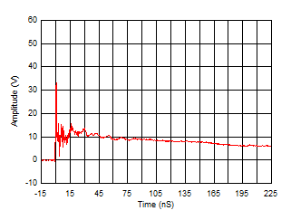
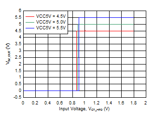
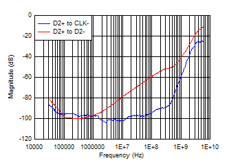
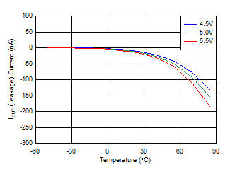
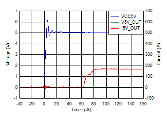
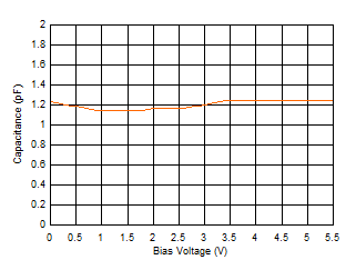
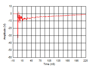
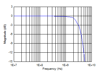
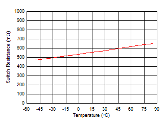
Iswitch at Approximately 55 mA
