ZHCS824D March 2012 – October 2015 TPD13S523
PRODUCTION DATA.
- 1 特性
- 2 应用
- 3 说明
- 4 修订历史记录
- 5 Pin Configuration and Functions
- 6 Specifications
-
7 Detailed Description
- 7.1 Overview
- 7.2 Functional Block Diagram
- 7.3
Feature Description
- 7.3.1 IEC 61000-4-2 Protection
- 7.3.2 Single-Chip ESD Solution
- 7.3.3 On-Chip 5-V Load Switch
- 7.3.4 Supports UTILITY Line Protection
- 7.3.5 < 0.05-pF Differential Capacitance Between TMDS Pairs
- 7.3.6 Industry Standard Package and Space-Saving Package
- 7.3.7 Supports Data Rates in Excess of 3.4 Gbps
- 7.3.8 RDYN = 0.5 Ω
- 7.3.9 Commercial Temperature Range
- 7.4 Device Functional Modes
- 8 Application and Implementation
- 9 Power Supply Recommendations
- 10Layout
- 11器件和文档支持
- 12机械、封装和可订购信息
10 Layout
10.1 Layout Guidelines
The TPD13S523 device offers little or no signal distortion during normal operation due to low I/O capacitance and ultra-low leakage current specifications. In the event of an ESD stress, this device ensures that the core circuitry is protected and the system is functioning properly. For proper operation, the following layout and design guidelines should be followed:
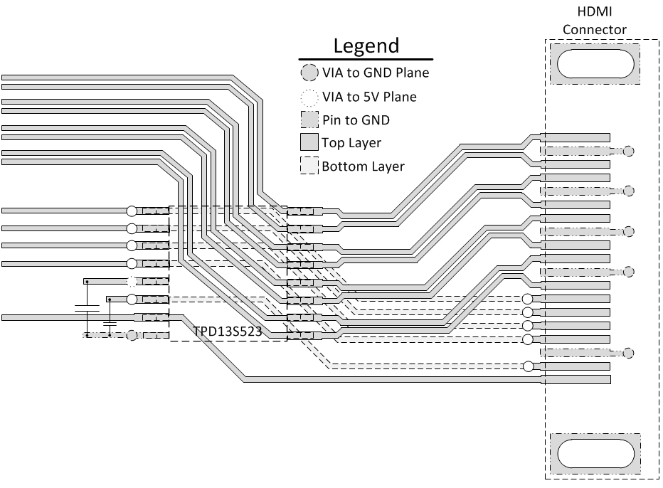
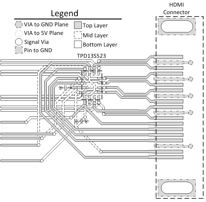
- Place the TPD13S523 as close to the connector as possible. This allows the TPD13S523 to remove the energy associated with ESD strike before it reaches the internal circuitry of the system board.
- Place two 0.1-μF capacitors very close to the 5V_SUPPLY and 5V_OUT pins. These capacitors will help limit the noise at the 5V_OUT power line, and also help with system level ESD protection.
- Ensure that there is enough metallization for the GND pad. During normal operation, the TPD13S523 ESD pins consume ultra-low leakage current. During the ESD event, GND pin will see multiple amps of current. A sufficient current path enables safe discharge of all the energy associated with the ESD strike.
- The critical routing paths for HDMI interface are the high-speed TMDS lines. With the PW package, all the TMDS lines (pin Dxx) can be routed in a single signal plane and still maintain the differential coupling and trace symmetry. This helps reduce the overall board manufacturing cost. The slow speed control lines can be routed in another signal layer through vias.
- If the UTILITY or any other pin is not utilizied, tie the pin to a ground rather than leave floating. Use a 75-Ω resistor to protect against shorts to ground.
10.2 Layout Examples
 Figure 14. TPD13S523PWR Layout Example 13-Line HDMI Protection
 Figure 15. TPD13S523RSVR Layout Example 13-Line HDMI Protection