ZHCS824D March 2012 – October 2015 TPD13S523
PRODUCTION DATA.
- 1 特性
- 2 应用
- 3 说明
- 4 修订历史记录
- 5 Pin Configuration and Functions
- 6 Specifications
-
7 Detailed Description
- 7.1 Overview
- 7.2 Functional Block Diagram
- 7.3
Feature Description
- 7.3.1 IEC 61000-4-2 Protection
- 7.3.2 Single-Chip ESD Solution
- 7.3.3 On-Chip 5-V Load Switch
- 7.3.4 Supports UTILITY Line Protection
- 7.3.5 < 0.05-pF Differential Capacitance Between TMDS Pairs
- 7.3.6 Industry Standard Package and Space-Saving Package
- 7.3.7 Supports Data Rates in Excess of 3.4 Gbps
- 7.3.8 RDYN = 0.5 Ω
- 7.3.9 Commercial Temperature Range
- 7.4 Device Functional Modes
- 8 Application and Implementation
- 9 Power Supply Recommendations
- 10Layout
- 11器件和文档支持
- 12机械、封装和可订购信息
6 Specifications
6.1 Absolute Maximum Ratings
TA = –40°C to 85°C (1)| MIN | MAX | UNIT | ||
|---|---|---|---|---|
| VCC voltage tolerance | 5V_SUPPLY | –0.3 | 6 | V |
| IO voltage tolerance | Connector pins(2) | –0.3 | 6 | V |
| IEC 61000-4-5 peak current (8/20 µs) | Connector pins(2) | 3 | A | |
| IEC 61000-4-5 peak power (8/20 µs) | Connector pins(2) | 30 | W | |
| Storage temperature, Tstg | –65 | 125 | °C | |
(1) Stresses beyond those listed under Absolute Maximum Ratings may cause permanent damage to the device. These are stress ratings only, which do not imply functional operation of the device at these or any other conditions beyond those indicated under Recommended Operating Conditions. Exposure to absolute-maximum-rated conditions for extended periods may affect device reliability.
(2) Connector pins are Dx+, Dx–, CTRLx, and 5V_OUT
6.2 ESD Ratings
| VALUE | UNIT | |||
|---|---|---|---|---|
| V(ESD) | Electrostatic discharge | Human body model (HBM), per ANSI/ESDA/JEDEC JS-001(1) | ±2000 | V |
| Charged device model (CDM), per JEDEC specification JESD22-C101(2) | ±500 | |||
| IEC 61000-4-2 Contact Discharge | ±12000 | |||
| IEC 61000-4-2 Air-gap Discharge | ±14000 | |||
(1) JEDEC document JEP155 states that 500-V HBM allows safe manufacturing with a standard ESD control process.
(2) JEDEC document JEP157 states that 250-V CDM allows safe manufacturing with a standard ESD control process.
6.3 Recommended Operating Conditions
TA = –40°C to 85°C| MIN | MAX | UNIT | ||
|---|---|---|---|---|
| VCC Voltage | 5V_SUPPLY | 4.5 | 5.5 | V |
| IO voltage at external signal pins | Signal Pins(1) | –0.3 | 5.5 | V |
| Operating free-air temperature | –40 | 85 | °C | |
(1) External Signal pins are Dx+, Dx–, CTRLx, and 5V_OUT
6.4 Thermal Information
| THERMAL METRIC(1) | TPD13S523 | UNIT | ||
|---|---|---|---|---|
| PW [TSSOP] | RSV [UQFN] | |||
| 16 PINS | 16 PINS | |||
| RθJA | Junction-to-ambient thermal resistance | 119.9 | 153.2 | °C/W |
| RθJC(top) | Junction-to-case (top) thermal resistance | 54.5 | 70.9 | °C/W |
| RθJB | Junction-to-board thermal resistance | 65.0 | 74.7 | °C/W |
| ψJT | Junction-to-top characterization parameter | 9.7 | 2.9 | °C/W |
| ψJB | Junction-to-board characterization parameter | n/a | 74.7 | °C/W |
| RθJC(bot) | Junction-to-case (bottom) thermal resistance | n/a | n/a | °C/W |
(1) For more information about traditional and new thermal metrics, see the Semiconductor and IC Package Thermal Metrics application report, SPRA953.
6.5 Electrical Characteristics
TA = –40°C to 85°C (unless otherwise noted)| PARAMETER | TEST CONDITIONS | MIN | TYP | MAX | UNIT | |
|---|---|---|---|---|---|---|
| LOAD SWITCH | ||||||
| ICC | Supply current at 5V_SUPPLY | 5V_SUPPLY =5V, 5V OUT = Open | 6.5 | 7 | 10 | µA |
| ISC | Short-circuit current at 5V_OUT | 5V_SUPPLY =5V, 5V_OUT = GND | 100 | 116 | 147 | mA |
| IBACKDRIVE | Reverse leakage current at 5VOUT | 5V_SUPPLY =0V, 5V_OUT = 5 V | 0.01 | 0.69 | µA | |
| VDROP | 5V_OUT output voltage drop | 5V_SUPPLY =5V, I5V_OUT = 55 mA | 170 | 205 | mV | |
| CONNECTOR PINS | ||||||
| VRWM | Reverse stand-off voltage | 5.5 | V | |||
| VCLAMP | Clamp voltage with ESD strike | Ipp = 1 A, 8/20 μs(1) | 13 | V | ||
| Ipp = 3 A, 8/20 μs(1) | 15 | |||||
| IIO | Leakage current through external signal pins(3) | 5V_SUPPLY =5V, VIO = 5 V | 2 | 7 | 65 | nA |
| IOFF | Current from IO Port to supply pins when powered down through signal pins(2) | 5V_SUPPLY = 0 V, VIO = 2.5 V | 1 | 5 | 44 | nA |
| VF | Diode forward voltage through external signal pins(3); lower clamp diode | ID = 8 mA | 0.7 | 0.85 | 0.95 | V |
| RDYN | Dynamic resistance of ESD clamps external pins(2) | Pin to ground(3) | 0.5 | Ω | ||
| CIO_TMDS | IO capacitance Dx+, Dx– pins to GND | 5V_SUPPLY = 5 V, VIO = 2.5 V; ƒ = 1 MHz |
1 | pF | ||
| ΔCIO_TMDS | Differential capacitance for the Dx+, Dx– lines | 5V_SUPPLY = 5 V, VIO = 2.5 V; ƒ = 1 MHz |
0.05 | pF | ||
| CIO_CONTROL | CTRLx pin capacitance | 5V_SUPPLY = 5 V, VIO = 2.5 V; ƒ = 1 MHz |
1 | pF | ||
| VBR | Break-down voltage through signal pins(2) | IIO = 1 mA | 6 | V | ||
(1) Non-repetitive current pulse of an 8/20 µs exponentially decaying waveform according to IEC 61000-4-5.
(2) Signal pins are Dx+, Dx–, and CTRLx.
(3) Extraction of RDYN using least squares fit of TLP characteristics between I=1A AND I=10A.
6.6 Typical Characteristics
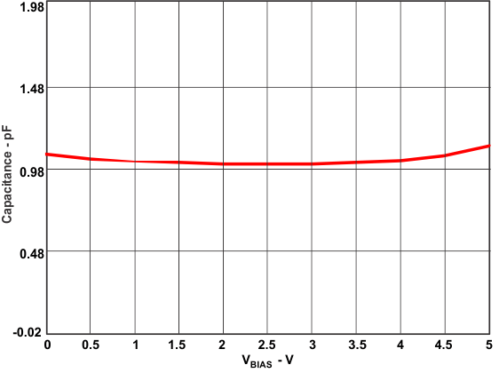 Figure 1. Pin Capacitance
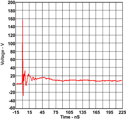 Figure 3. IEC Positive Clamping Waveform Using 8-kV Contact
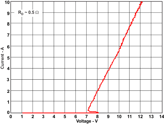 Figure 5. TLP Plot On Connector Pins
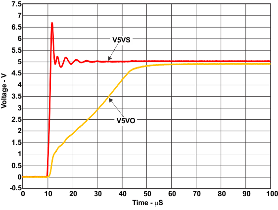
| CIN = 1 µF | COUT = 1µF | ISWITCH = 55 mA |
| TA = 25°C |
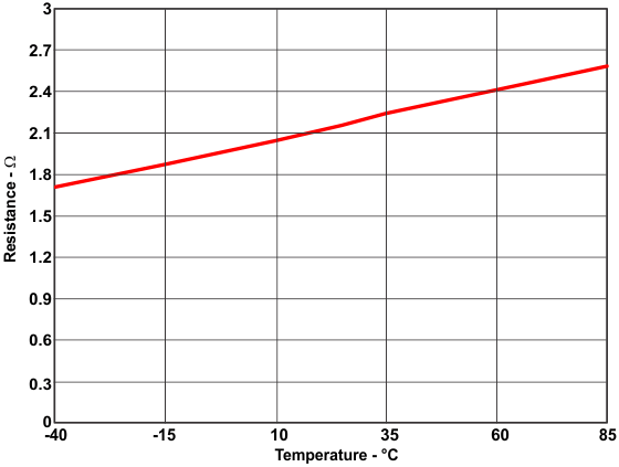 Figure 9. Load Switch Resistance vs Temperature
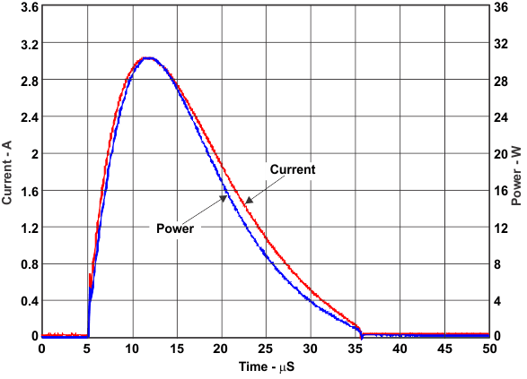 Figure 2. IEC 61000-4-5 (Surge) IPP and PPP Waveform
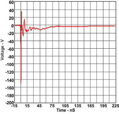 Figure 4. IEC Negative Clamping Waveform Using –8-kV Contact
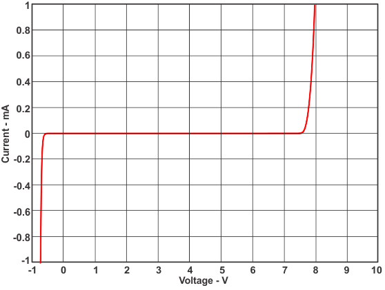 Figure 6. IV Curve On Signal Pins
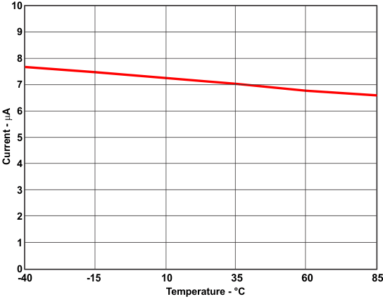
| 5V_SUPPLY = 5 V | 5V_OUT = Open |