ZHCS820E February   2012  – September 2023 TPD1E10B09

PRODUCTION DATA  

  1.   1
  2. 特性
  3. 应用
  4. 说明
  5. Revision History
  6. Pin Configuration and Functions
  7. Specifications
    1. 6.1 Absolute Maximum Ratings
    2. 6.2 ESD Ratings
    3. 6.3 Recommended Operating Conditions
    4. 6.4 Thermal Information
    5. 6.5 Electrical Characteristics
    6. 6.6 Typical Characteristics
  8. Detailed Description
    1. 7.1 Overview
    2. 7.2 Functional Block Diagram
    3. 7.3 Feature Description
    4. 7.4 Device Functional Modes
  9. Application and Implementation
    1. 8.1 Application Information
    2. 8.2 Typical Application
      1. 8.2.1 Design Requirements
      2. 8.2.2 Detailed Design Procedure
      3. 8.2.3 Application Curves
    3. 8.3 Power Supply Recommendations
    4. 8.4 Layout
      1. 8.4.1 Layout Guidelines
      2. 8.4.2 Layout Example
  10. Device and Documentation Support
    1. 9.1 接收文档更新通知
    2. 9.2 支持资源
    3. 9.3 Trademarks
    4. 9.4 静电放电警告
    5. 9.5 术语表
  11. 10Mechanical, Packaging, and Orderable Information

封装选项

机械数据 (封装 | 引脚)
散热焊盘机械数据 (封装 | 引脚)
订购信息

Typical Application

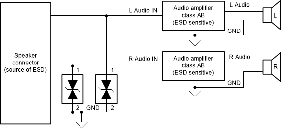
A system with a human interface is vulnerable to large system-level ESD strikes that standard ICs cannot survive. TVS ESD protection diodes are typically used to suppress ESD at these connectors. TPD1E10B09 is a single-channel ESD protection device containing back-to-back TVS diodes, which is typically used to provide a path to ground for dissipating ESD events on bidirectional signal lines between a human interface connector and a system. As the current from ESD passes through the device, only a small voltage drop is present across the diode structure. This is the voltage presented to the protected IC. The low RDYN of the triggered TVS holds this voltage, VCLAMP, to a tolerable level to the protected IC.
GUID-1F6760BE-8A6B-4E07-914A-B6F1E788AA7D-low.gifFigure 8-1 Typical Application Schematic