SLLS684I July 2006 – March 2016 TPD2E001
PRODUCTION DATA.
- 1 Features
- 2 Applications
- 3 Description
- 4 Revision History
- 5 Pin Configuration and Functions
- 6 Specifications
- 7 Detailed Description
- 8 Application and Implementation
- 9 Power Supply Recommendations
- 10Layout
- 11Device and Documentation Support
- 12Mechanical, Packaging, and Orderable Information
封装选项
机械数据 (封装 | 引脚)
散热焊盘机械数据 (封装 | 引脚)
订购信息
8 Application and Implementation
NOTE
Information in the following applications sections is not part of the TI component specification, and TI does not warrant its accuracy or completeness. TI’s customers are responsible for determining suitability of components for their purposes. Customers should validate and test their design implementation to confirm system functionality.
8.1 Application Information
TPD2E001 is a diode array type Transient Voltage Suppressor (TVS) which is typically used to provide a path to ground for dissipating ESD events on hi-speed signal lines between a human interface connector and a system. As the current from ESD passes through the TVS, only a small voltage drop is present across the diode. This is the voltage presented to the protected IC. The low RDYN of the triggered TVS holds this voltage, VCLAMP, to a tolerable level to the protected IC.
8.2 Typical Application
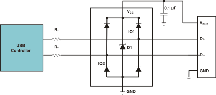
 Figure 5. Typical USB Application Diagram
8.2.1 Design Requirements
For this design example, a single TPD2E001 is used to protect all pins of a USB 2.0 connector.
Given the USB application, Table 1 shows the Design Parameters:
Table 1. Design Parameters
| DESIGN PARAMETER | VALUE |
|---|---|
| Signal range on IO1, and IO2 | 0 V to 5 V |
| Signal voltage range on VCC | 0 V to 5 V |
| Operating frequency | 240 MHz |
8.2.2 Detailed Design Procedure
To begin the design process, some parameters must be decided upon; the designer needs to know the following:
- Signal voltage range on all the protected lines
- Operating frequency
The VCC pin can be connected in two different ways:
- If the VCC pin is connected to the system power supply, the TPD2E001 works as a transient suppressor for any signal swing above VCC + VF. A 0.1-μF capacitor on the device VCC pin is recommended for ESD bypass.
- If the VCC pin is not connected to the system power supply, the TPD2E001 can tolerate higher signal swing in the range up to 10 V. Please note that a 0.1-μF capacitor is still recommended at the VCC pin for ESD bypass.
8.2.2.1 Signal Range on IO1 and IO2 and VCC Pins
The TPD2E001 has 2 IO pins which support 0 to either 10 V or VCC + Vforward (depending on if the VCC pin is connected to a VCC line or has a 0.1 µF capacitor to ground).