SLLS684I July 2006 – March 2016 TPD2E001
PRODUCTION DATA.
- 1 Features
- 2 Applications
- 3 Description
- 4 Revision History
- 5 Pin Configuration and Functions
- 6 Specifications
- 7 Detailed Description
- 8 Application and Implementation
- 9 Power Supply Recommendations
- 10Layout
- 11Device and Documentation Support
- 12Mechanical, Packaging, and Orderable Information
封装选项
机械数据 (封装 | 引脚)
散热焊盘机械数据 (封装 | 引脚)
订购信息
5 Pin Configuration and Functions
DRY Package
6-Pin USON
Top View

N.C. – Not internally connected
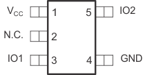
DRL Package
5-Pin SOT
Top View

N.C. – Not internally connected
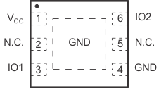
DRS Package
6-Pin WSON
Top View

N.C. – Not internally connected
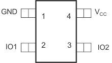
DZD Package
4-Pin SOP
Top View

Pin Functions
| PIN | DESCRIPTION | ||||
|---|---|---|---|---|---|
| NAME | DRY NO. |
DRL NO. |
DRS NO. |
DZD NO. |
|
| EP | — | — | EP | — | Exposed pad. Connect to GND. |
| GND | 4 | 4 | 4 | 1 | Ground |
| IOx | 3, 6 | 3, 5 | 3, 6 | 2, 3 | ESD-protected channel |
| N.C. | 2, 5 | 2 | 2, 5 | — | No connection. Not internally connected. |
| VCC | 1 | 1 | 1 | 4 | Power-supply input. Bypass VCC to GND with a 0.1-μF ceramic capacitor. |