SLVS796I September 2008 – March 2016 TPD2E007
PRODUCTION DATA.
6 Specifications
6.1 Absolute Maximum Ratings
over operating free-air temperature range (unless otherwise noted)(1)(1) Stresses beyond those listed under Absolute Maximum Ratings may cause permanent damage to the device. These are stress ratings only, and functional operation of the device at these or any other conditions beyond those indicated in the operational sections of the specifications is not implied. Exposure to absolute maximum-rated conditions for extended periods may affect device reliability.
6.2 ESD Ratings
| VALUE | UNIT | ||||
|---|---|---|---|---|---|
| V(ESD) | Electrostatic discharge | Human body model (HBM), per ANSI/ESDA/JEDEC JS-001, all pins(1) | ±15000 | V | |
| Charged device model (CDM), per JEDEC specification JESD22-C101, all pins(2) | ±1500 | ||||
(1) JEDEC document JEP155 states that 500-V HBM allows safe manufacturing with a standard ESD control process.
(2) JEDEC document JEP157 states that 250-V CDM allows safe manufacturing with a standard ESD control process.
6.3 ESD Ratings: Surge Protection
| VALUE | UNIT | ||||
|---|---|---|---|---|---|
| V(ESD) | Electrostatic discharge | IEC 61000-4-2 ESD ratings | Contact | ±8000 | V |
| Air gap | ±15000 | ||||
6.4 Recommended Operating Conditions
over operating free-air temperature range (unless otherwise noted)| MIN | NOM | MAX | UNIT | ||
|---|---|---|---|---|---|
| VIO | Operating voltage | –13 | 13 | V | |
| Operating temperature | –40 | 85 | °C | ||
6.5 Thermal Information
| THERMAL METRIC(1) | TPD2E007 | UNIT | ||
|---|---|---|---|---|
| DCK (SOT) | YFM (PicoStar) | |||
| 3 PINS | 4 PINS | |||
| RθJA | Junction-to-ambient thermal resistance | 251.9 | 175.9 | °C/W |
| RθJC(top) | Junction-to-case (top) thermal resistance | 115.4 | 39.2 | °C/W |
| RθJB | Junction-to-board thermal resistance | 42.4 | 28.7 | °C/W |
| ψJT | Junction-to-top characterization parameter | 9.4 | 8.3 | °C/W |
| ψJB | Junction-to-board characterization parameter | 42.2 | 28.7 | °C/W |
| RθJC(bot) | Junction-to-case (bottom) thermal resistance | N/A | N/A | °C/W |
(1) For more information about traditional and new thermal metrics, see the Semiconductor and IC Package Thermal Metrics application report, SPRA953.
6.6 Electrical Characteristics
TA = –40°C to 85°C (unless otherwise noted)| PARAMETER | TEST CONDITIONS | MIN | TYP(1) | MAX | UNIT | |
|---|---|---|---|---|---|---|
| VBRF | Break-down voltage, pin 1 or 2 to GND | IIO = 10 mA | 14 | V | ||
| VBRR | Break-down voltage, GND to pin 1 or 2 | IIO = 10 mA | 14 | V | ||
| IIO | Channel leakage current | 20 | 50 | nA | ||
| Rd | Dynamic resistance | 3.5 | Ω | |||
| CIN | Channel input capacitance | VIO = 2.5 V; ƒ = 10 MHz | 10 | 15 | pF | |
(1) Typical values are at VCC = 5 V and TA = 25°C.
6.7 Typical Characteristics
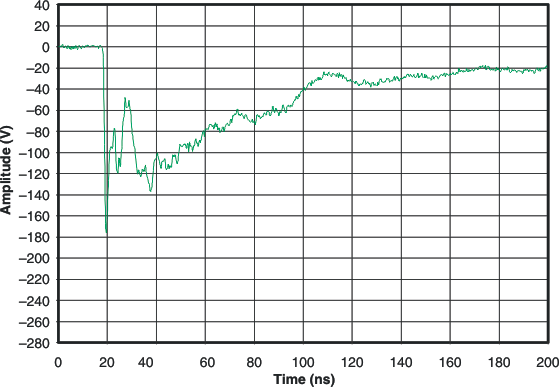
IEC Clamping Waveforms (20 ns/div) Figure 1. 8-kV Contact
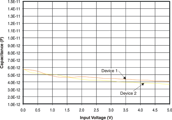
 Figure 3. Capacitance vs Input Voltage at TA = 27°C
 Figure 2. –8-kV Contact
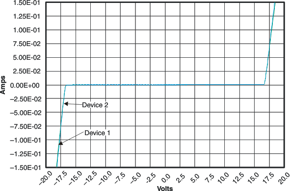
 Figure 4. Diode Breakdown Voltage Data at TA = 27°C