SLVSC77D August   2013  – April 2016 TPD2E1B06

PRODUCTION DATA.  

  1. Features
  2. Applications
  3. Description
  4. Revision History
  5. Pin Configuration and Functions
  6. Specifications
    1. 6.1 Absolute Maximum Ratings
    2. 6.2 ESD Ratings
    3. 6.3 Recommended Operating Conditions
    4. 6.4 Thermal Information
    5. 6.5 Electrical Characteristics
    6. 6.6 Typical Characteristics
  7. Detailed Description
    1. 7.1 Overview
    2. 7.2 Functional Block Diagram
    3. 7.3 Feature Description
    4. 7.4 Device Functional Modes
  8. Application and Implementation
    1. 8.1 Application Information
    2. 8.2 Typical Application
      1. 8.2.1 Design Requirements
      2. 8.2.2 Detailed Design Procedure
      3. 8.2.3 Application Curves
  9. Power Supply Recommendations
  10. 10Layout
    1. 10.1 Layout Guidelines
    2. 10.2 Layout Examples
  11. 11Device and Documentation Support
    1. 11.1 Community Resources
    2. 11.2 Trademarks
    3. 11.3 Electrostatic Discharge Caution
    4. 11.4 Glossary
  12. 12Mechanical, Packaging, and Orderable Information

封装选项

机械数据 (封装 | 引脚)
散热焊盘机械数据 (封装 | 引脚)
订购信息

10 Layout

10.1 Layout Guidelines

• The optimum placement of the TPD2E1B06 is as close to the connector as possible. EMI during an ESD event can couple from the trace being struck to other nearby unprotected traces, resulting in early system failures. The printed-circuit board (PCB) designer must minimize the possibility of EMI coupling by keeping any unprotected traces away from the protected traces, which are between the TVS and the connector.

• Route the protected traces as straight as possible.

• Avoid sharp corners on the protected traces. Electric fields tend to build up on corners, increasing EMI coupling.

• Use thick and short traces for the ground pins

10.2 Layout Examples
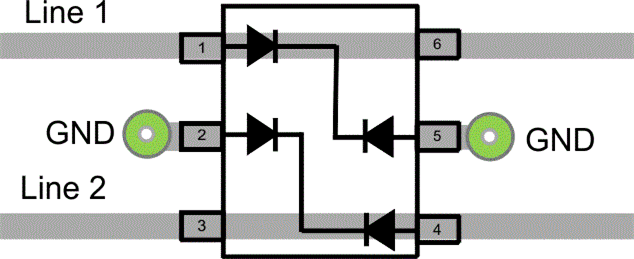
TPD2E1B06 app2_lvsc77.gif Figure 13. Routing Option 1
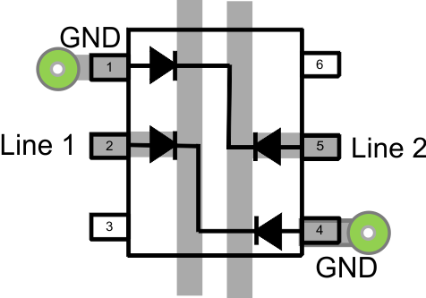
TPD2E1B06 3354.gif Figure 14. Routing Option 2