ZHCSO74C September   2009  – January 2023 TPD2S017

PRODUCTION DATA  

  1. 特性
  2. 应用
  3. 说明
  4. Revision History
  5. Pin Configuration and Functions
  6. Specifications
    1. 6.1 Absolute Maximum Ratings
    2. 6.2 ESD Ratings
    3. 6.3 Recommended Operating Conditions
    4. 6.4 Thermal Information
    5. 6.5 Electrical Characteristics
    6. 6.6 Dissipation Ratings
    7. 6.7 Typical Characteristics
  7. Detailed Description
    1. 7.1 Overview
    2. 7.2 Functional Block Diagram
    3. 7.3 Feature Description
    4. 7.4 Device Functional Modes
  8. Application and Implementation
    1. 8.1 Application Information
    2. 8.2 Typical Application
      1. 8.2.1 Design Requirements
      2. 8.2.2 Detailed Design Procedure
      3. 8.2.3 Application Curves
  9. Power Supply Recommendations
  10. 10Layout
    1. 10.1 Layout Guidelines
    2. 10.2 Layout Example
  11. 11Device and Documentation Support
    1. 11.1 接收文档更新通知
    2. 11.2 支持资源
    3. 11.3 Trademarks
    4. 11.4 静电放电警告
    5. 11.5 术语表
  12. 12Mechanical, Packaging, and Orderable Information

封装选项

机械数据 (封装 | 引脚)
散热焊盘机械数据 (封装 | 引脚)
订购信息

Typical Characteristics

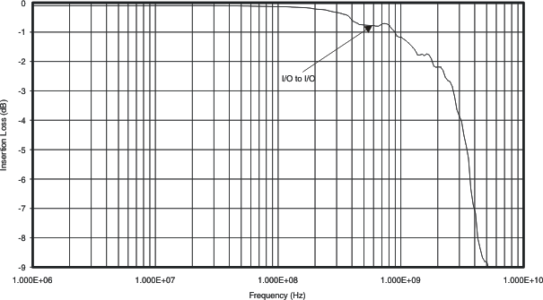
GUID-8445B4FC-7B75-417E-9912-D0854B013A39-low.gifFigure 6-1 Insertion Loss Data (S21)
GUID-5DE6B685-53EC-4608-AC22-0BDC3D57E75A-low.gif
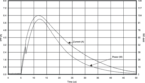
Figure 6-3 Peak Pulse Waveforms Ch2_In, PUT with respect to GND, VCC = 5 V
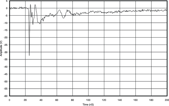
GUID-23F783A5-59F6-414A-8058-0B16239B4A99-low.gifFigure 6-5 IEC Clamping Waveforms –8 kV Contact, 1 GHz Bandwidth
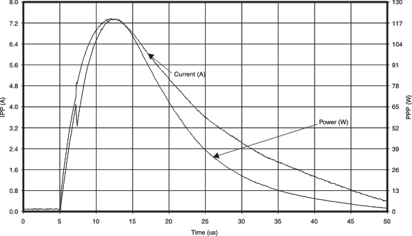
GUID-52A43A7D-F75E-4FB2-AD8E-E0D3505B6CD8-low.gifFigure 6-2 Peak Pulse Waveforms Ch1_Out, PUT with respect to GND, VCC = 5 V
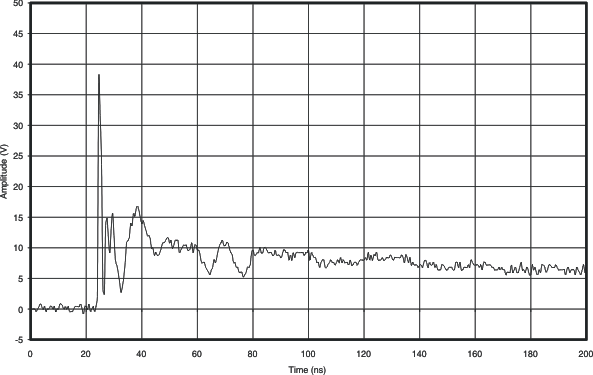
GUID-C905A080-D654-4949-A6BB-F4EC8A1051A9-low.gifFigure 6-4 IEC Clamping Waveforms 8 kV Contact, 1 GHz Bandwidth