ZHCSGS3 April 2017 TPD2S300
PRODUCTION DATA.
- 1 特性
- 2 应用
- 3 说明
- 4 修订历史记录
- 5 Pin Configuration and Functions
- 6 Specifications
-
7 Detailed Description
- 7.1 Overview
- 7.2 Functional Block Diagram
- 7.3
Feature Description
- 7.3.1 2-Channels of Short-to-VBUS Overvoltage Protection (CC1, CC2 Pins): 24-VDC Tolerant
- 7.3.2 2-Channels of IEC61000-4-2 ESD Protection (CC1, CC2 Pins)
- 7.3.3 Low Quiescent Current: 3.23 µA (Typical), VPWR, VM = 3.3 V
- 7.3.4 CC1, CC2 Overvoltage Protection FETs 200 mA Capable for Passing VCONN Power
- 7.3.5 CC Dead Battery Resistors Integrated for Handling Dead Battery Use Case in Mobile Devices
- 7.3.6 1.4-mm × 1.4-mm WCSP Package
- 7.4 Device Functional Modes
- 8 Application and Implementation
- 9 Power Supply Recommendations
- 10Layout
- 11器件和文档支持
- 12机械、封装和可订购信息
8 Application and Implementation
NOTE
Information in the following applications sections is not part of the TI component specification, and TI does not warrant its accuracy or completeness. TI’s customers are responsible for determining suitability of components for their purposes. Customers should validate and test their design implementation to confirm system functionality.
8.1 Application Information
The TPD2S300 provides 2-channels of Short-to-VBUS overvoltage protection for the CC1 and CC2 pins of the USB Type-C connector, and 2-channels of IEC ESD protection for the CC1 and CC2 pins of the USB Type-C connector. Care must be taken to insure that the TPD2S300 provides adequate system protection as well as insuring that proper system operation is maintained. The following application examples explain how to properly design the TPD2S300 into a USB Type-C system.
8.2 Typical Application
8.2.1 Smart-Phone Application
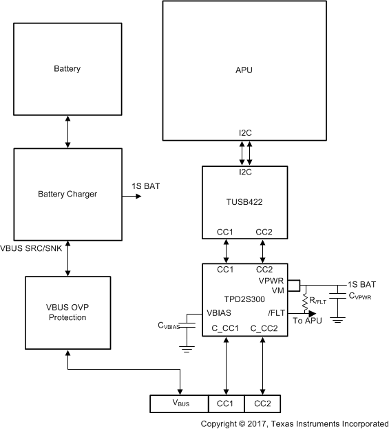 Figure 21. TPD2S300 Typical Application Diagram
8.2.1.1 Design Requirements
In this application example, we use the TPD2S300 to protect a USB Type-C port in a smart-phone application. In this application, the smart-phone needs USB2.0 support and 20-V, 2-A charging. Because 20 V is required, USB-PD needs to be used in this application to achieve this, as USB Type-C alone cannot support higher than 5 V. In order to add USB-PD operation in a smart-phone application, the TUSB422 is used. This device is a TCPCi that adds the USB Type C and USB-PD physical layer required to run USB PD over the USB Type-C connector. This device can be connected to the APU in the system through I2C, and the APU can run the USB-PD code.
With USB-C with 20-V PD being used, a Short-to-VBUS event can occur in the system. This short can affect both the CC and SBU pins. However, in this application, since only USB2.0 is required, the SBU pin is not used. Therefore, only CC Short-to-VBUS protection is required to adequately protect the TUSB422 and the system. The CC pins also needs IEC61000-4-2 system level ESD protection. Additionally, with this application being a smart-phone, board space is crucial; a small protection device is required. Therefore, with these application requirements, the TPD2S300 is used, a single-chip solution which integrates all the protection requirements needed for the CC pins in this application.
Table 2 shows the TPD2S300 design parameters for this application.
Table 2. Design Parameters
| DESIGN PARAMETER | EXAMPLE VALUE |
|---|---|
| VBUS nominal operating voltage | 20 V |
| Short-to-VBUS tolerance for the CC pins | 24 V |
| VBIAS nominal capacitance | 0.1 µF |
| Dead battery charging | 40 W |
| TPD2S300 VPWR and VM power source | 3.3-V LDO or 1S battery |
| Quiescent current required for protection device | ≤ 20 µA |
| VCONN requirement | VCONN not required |
| Maximum ambient temperature requirement | 85°C |
8.2.1.2 Detailed Design Procedure
8.2.1.2.1 VBIAS Capacitor Selection
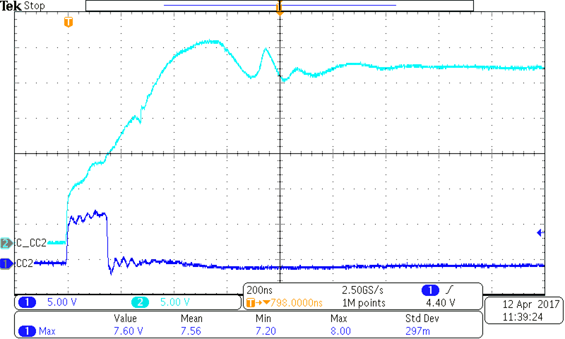
As noted in the Recommended Operating Conditions table, a minimum of 35-VBUS rated capacitor is required for the VBIAS pin, and a 50-VBUS capacitor is recommended. The VBIAS capacitor is in parallel with the central IEC diode clamp integrated inside the TPD2S300. A forward biased hiding diode connects the VBIAS pin to the C_CCx pins. Therefore, when a Short-to-VBUS event occurs at 20 V, 20-VBUS minus a forward biased diode drop is exposed to the VBIAS pin. Additionally, during the Short-to-VBUS event, ringing can occur almost double the settling voltage of 20 V, allowing a potential 40 V to be exposed to the C_CCx pins. However, the internal IEC clamps limits the voltage exposed to the C_CCx pins to around 30 V. Therefore, at least 35-VBUS capacitor is required to insure the VBIAS capacitor does not get destroyed during Short-to-VBUS events.
A 50-V, X7R capacitor is recommended, however. This is to further improve the derating performance of the capacitors. When the voltage across a real capacitor is increased, its capacitance value derates. The more the capacitor derates, the greater than 2x ringing can occur in the Short-to-VBUS RLC circuit. 50-V X7R capacitors have great derating performance, allowing for the best Short-to-VBUS performance of the TPD2S300.
Additionally, the VBIAS capacitor helps pass IEC 61000-4-2 ESD strikes. The more capacitance present, the better the IEC performance. So the less the VBIAS capacitor derates, the better the IEC performance. Table 3 shows the real capacitors recommended to achieve the best performance with the TPD2S300.
Table 3. Design Parameters
| CAPACITOR SIZE | PART NUMBER |
|---|---|
| 0402 | CC0402KRX7R9BB104 |
| 0603 | GRM188R71H104KA93D |
8.2.1.2.2 Dead Battery Operation
For this application, we want to support 40-W dead battery operation; when the smart-phone is out of battery, we still want to charge the laptop at 20 V and 2 A. This means that the USB PD Controller must receive power in dead battery mode. This means a dead battery LDO must be present in the system to power the TUSB422 and the APU controlling TUSB422 during dead battery. Or, the system PMIC must be able to provide the 1S battery to the APU and TUSB422 during dead battery conditions.
The TPD2S300s OVP FETs remain OFF when it is unpowered in order to insure in a dead battery situation proper protection is still provided to the PD controller or TCPCi in the system, in this case the TUSB422. However, when the OVP FETs are OFF, this isolates the TUSB422's dead battery resistors from the USB Type-C ports CC pins. A USB Type-C power adaptor must see the RD pull-down dead battery resistors on the CC pins or it does not turn on VBUS to provide power. Since the TUSB422's dead battery resistors are isolated from the USB Type-C connector's CC pins, the TPD2S300 integrates dead battery resistors on its C_CCx pins. The TPD2S300 exposes these pins when it is unpowered.
Once the power adaptor sees the TPD2S300's dead battery resistors, it applies 5 V on the VBUS pin. This provides power to the dead battery LDO or PMIC, allowing power to be applied to the APU and TUSB422 to turn them ON, and allowing the battery to begin to charge. However, this application requires 40-W charging in dead battery mode, so VBUS at 20 V and 2 A is required. USB PD negotiation is required to accomplish this, so the APU through the TUSB422 needs to be able to communicate on the CC pins. This means the TPD2S300 needs to be turned on in dead battery mode as well so the TUSB422 can be exposed to the CC lines. To accomplish this, it is critical that the TPD2S300 is powered by the same dead battery LDO or battery voltage as the APU and TUSB422 during dead battery. This way, the TPD2S300 is turned ON simultaneously with TUSB422.
It is critical that the TUSB422's dead battery resistors are also active on its CC pins for dead battery operation. Once the TPD2S300 receives power, removes its dead battery resistors and turns on its OVP FETs, RD pull-down resistors must be present on the CC line in order to guarantee the power adaptor stays connected. If RD is not present and the voltage on CC increases into the SRC.Open range, the power adaptor can interpret this as a port disconnect and remove VBUS.
Once this process has occured, the APU through the TUSB422 can start negotiating with the power adaptor through USB PD for higher power levels, allowing for 40W operation in dead battery mode.
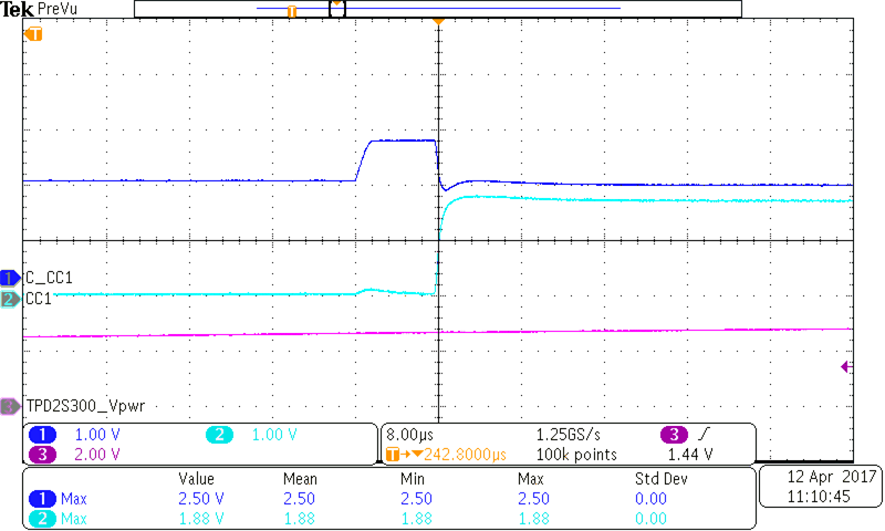
For more information on the TPD2S300 dead battery operation, see the CC Dead Battery Resistors Integrated for Handling Dead Battery Use Case in Mobile Devices section in the description section of the datasheet. Also, see Figure 22 for a waveform of the CC line when the TPD2300 is turning on and exposing RD dead battery resistors to the USB Type-C connector.
8.2.1.2.3 CC Line Capacitance
USB PD has a specification for the total amount of capacitance that is required for proper USB PD BMC operation on the CC lines. The specification from section 5.8.6 of the USB PD Specification is given in Table 4.
Table 4. USB PD cReceiver Specification
| NAME | DESCRIPTION | MIN | MAX | UNIT | COMMENT |
|---|---|---|---|---|---|
| cReceiver | CC receiver capacitance | 200 | 600 | pF | The DFP or UFP system shall have capacitance within this range when not transmitting on the line |
Therefore, the capacitance on the CC lines must stay in between 200 pF and 600 pF when USB PD is being used. Therefore, the combination of capacitances added to the system by the TUSB422, the TPD2S300, and any external capacitor must fall within these limits. Table 5 shows that with TUSB422 + TPD2S300, no external capacitor is required to meet the USB-PD specification.
Table 5. CC Line Capacitor Calculation
| CC Capacitance | MIN | MAX | UNIT | COMMENT |
|---|---|---|---|---|
| CC line target capacitance | 200 | 600 | pF | From the USB PD Specification section (cReceiver, section 5.8.6) |
| TUSB422 capacitance | 200 | 450 | pF | From the TUSB422 Datasheet |
| TPD2S300 capacitance | 30 | 120 | pF | From the Electrical Characteristics table |
| TUSB422 + TPD2S300 | 230 | 570 | pF | Meets USB PD cReceiver Specification |
8.2.1.2.4 FLT Pin Operation
A FLT pin is provided on the TPD2S300 to give the APU the ability to be notified that a Short-to-VBUS event occured. Once a Short-to-VBUS occurs on the C_CCx pins, the FLT pin is asserted in 1 µs (typical) so the PD controller can be notified quickly. If VBUS is being shorted to CC, it is recommended to respond to the event by forcing a detach in the USB PD controller to remove VBUS from the port. Although the USB Type-C port using the TPD2S300 is not damaged, as the TPD2S300 provides protection from these events, the other device connected through the USB Type-C Cable or any active circuitry in the cable can be damaged. Although shutting the VBUS off through a detach does not guarantee it stops the other device or cable from being damaged, it can mitigate any high current paths from causing further damage after the initial damage takes place. Additionally, even if the active cable or other device does have proper protection, the Short-to-VBUS event may corrupt a configuration in an active cable or in the other PD controller, so it is best to detach and reconfigure the port. Therefore, in this application it is recommended that the APU monitor the FLT pin for Short-to-VBUS faults.
8.2.1.2.5 VCONN Operation
In our current application example, VCONN is not required. Therefore, a 3.3-V source or 1S battery can be connected to the VPWR and VM pins of the TPD2S300 and provide adaqute resistance in order to support CC analog and USB PD operation over the CC lines. In fact, the CC OVP FETs resistance specifications are set to optimize the FET size and therefore the TPD2S300 size and still allow proper CC analog and USB PD operation. See the Electrical Characteristics table for the specific resistances of the CC OVP FETs.
8.2.1.2.6 Low Quiescent Current
Smart-Phone applications require low quiescent current to meet long battery life specifications to provide the best experience to end-users. The TPD2S300 is designed to have very low quiescent current in order to meet these requirements. The lower the voltage kept on the C_CCx lines, and the lower the voltage kept on the VPWR and VM pins, the lower the quiescent current is on the TPD2S300. If an LDO is used that keeps VPWR and VM limited to 3.3 V, then the maximum quiescent current on VPWR is 7 µA, and the maximum current on VM is 1 µA. If the 1S battery is connected to the VPWR and VM pins, such that the maximum voltage applied to VPWR and VM is 4.5 V, then the maximum quiescent current is going to be 12 µA for VPWR, and VM has 1 µA maximum. Therefore, our application can achieve a very low total quiescent current for protection with the TPD2S300, between 8 µA and 13 µA, depending on how the TPD2S300 is powered. For all details on quiescent current values, see the Electrical Characteristics table.
8.2.1.3 Application Curves

8.2.2 Laptop Application
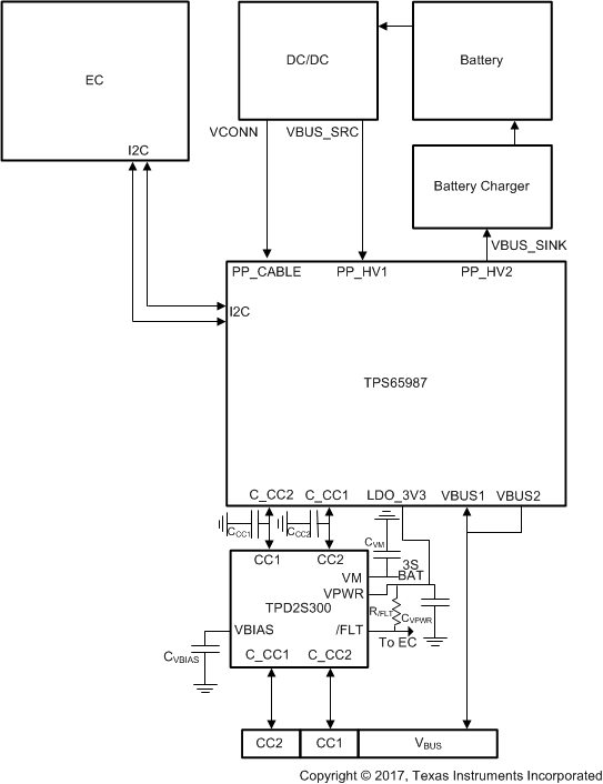 Figure 23. TPD2S300 Typical Application Diagram
8.2.2.1 Design Requirements
In this application example, we use the TPD2S300 to protect a USB Type-C port in a laptop application. In this application, the laptop needs USB3.0 support and 20-V, 5-A charging. Because 20 V is required, USB-PD needs to be used in this application to achieve this, as USB Type-C alone cannot support higher than 5 V. In order to add USB-PD operation in a laptop application, the TPS65987 is used. This device is a full-featured USB Type-C and USB PD controller that integrates all the analog and power paths needed to support 20-V, 5-A charging and USB3.0.
With USB-C with 20-V PD being used, a Short-to-VBUS event can occur in the system. This short can affect both the CC and SBU pins. However, in this application, since only USB3.0 is required, the SBU pin is not used. Therefore, only CC Short-to-VBUS protection is required to adequately protect TPS65987 and the system. The CC pins also need IEC61000-4-2 system level ESD protection. Additionally, with this application being a laptop, board space is crucial; a small protection device is required. Therefore, with these application requirements, the TPD2S300 is used, a single-chip solution which integrates all the protection requirements needed for the CC pins in this application.
Table 2 shows the TPD2S300 design parameters for this application.
Table 6. Design Parameters
| DESIGN PARAMETER | EXAMPLE VALUE |
|---|---|
| VBUS nominal operating voltage | 20 V |
| Short-to-VBUS tolerance for the CC pins | 24 V |
| VBIAS nominal capacitance | 0.1 µF |
| Dead battery charging | 100 W |
| TPD2S300 VPWR power source | 3.3-V LDO from TPS65987 |
| TPD2S300 VM power source | 3S or 4S Battery |
| VCONN requirement | 1-W VCONN required |
| Maximum ambient temperature requirement | 85°C |
8.2.2.2 Detailed Design Procedure
8.2.2.2.1 VBIAS Capacitor Selection
This VBIAS capacitor requirements for this application are identical to the Smart-Phone application; see the VBIAS Capacitor Selection section for more details.
8.2.2.2.2 Dead Battery Operation
For this application, we want to support 100-W dead battery operation; when the laptop is out of battery, we still want to charge the laptop at 20 V and 5 A. This means that the USB PD Controller must receive power in dead battery mode. The TPS65987 has its own built in LDO in order to supply the TPS65987 power from VBUS in a dead battery condition. The TPS65987 can also provide power to its flash during this condition through its LDO_3V3 pin.
The TPD2S300s OVP FETs remain OFF when it is unpowered in order to insure in a dead battery situation proper protection is still provided to the PD controller in the system, in this case the TPS65987. However, when the OVP FETs are OFF, this isolates the TPS65987's dead battery resistors from the USB Type-C ports CC pins. A USB Type-C power adaptor must see the RD pull-down dead battery resistors on the CC pins or it does not turn ON VBUS to provide power. Since the TPS65987s dead battery resistors are isolated from the USB Type-C connector's CC pins, the TPD2S300 integrates dead battery resistors on its C_CCx pins, and exposes them when the device is unpowered.
Once the power adaptor sees the TPD2S300's dead battery resistors, it applies 5 V on the VBUS pin. This provides power to the TPS65987, turning the PD controller on, and allowing the battery to begin to charge. However, this application requires 100-W charging in dead battery mode, so VBUS at 20 V and 5 A is required. USB PD negotiation is required to accomplish this, so the TPS65987 needs to be able to communicate on the CC pins. This means the TPD2S300 needs to be turned on in dead battery mode as well so the TPD65987's PD controller can be exposed to the CC lines. To accomplish this, it is critical that the TPD2S300 is powered by the TPS65987's internal LDO, the LDO_3V3 pin. This way, when the TPS65987 receives power on VBUS, the TPD2S300 is turned on simultaneously. Additionally, for low resistance VCONN support, the VM pin needs to be connected to the 3S battery, so TPD2S300 needs to be able to receive this voltage in the dead battery condition as well.
It is critical that the TPS65987's dead battery resistors are present; once the TPD2S300 receives power, removes its dead battery resistors and turns on its OVP FETs, RD pull-down resistors must be present on the CC line in order to guarantee the power adaptor stays connected. If RD is not present and the voltage on CC increases to Src.Open, the power adaptor can interpret this as a disconnect and remove VBUS.
Also, it is important that the TPS65987's dead battery resistors are present so it properly boots up in dead battery operation with the correct voltages on its CC pins.
Once this process has occurred, the TPS65987 can start negotiating with the power adaptor through USB PD for higher power levels, allowing 100-W operation in dead battery mode.
For more information on the TPD2S300 dead battery operation, see the CC Dead Battery Resistors Integrated for Handling Dead Battery Use Case in Mobile Devices section in the description section of the datasheet. Also, see Figure 22 for a waveform of the CC line when the TPD2S300 is turning on and exposing the TPS65987's dead battery resistors to the USB Type-C connector.
8.2.2.2.3 CC Line Capacitance
USB PD has a specification for the total amount of capacitance that is required for proper USB PD BMC operation on the CC lines. The specification from section 5.8.6 of the USB PD Specification is given in Table 4.
Table 7. USB PD cReceiver Specification
| NAME | DESCRIPTION | MIN | MAX | UNIT | COMMENT |
|---|---|---|---|---|---|
| cReceiver | CC receiver capacitance | 200 | 600 | pF | The DFP or UFP system shall have capacitance within this range when not transmitting on the line |
Therefore, the capacitance on the CC lines must stay in between 200 pF and 600 pF when USB PD is being used. Therefore, the combination of capacitances added to the system by the TPS65987, the TPD2S300, and any external capacitor must fall within these limits. Table 5 shows the analysis involved in choosing the correct external CC capacitor for this system, and shows that an external CC capacitor is required.
Table 8. CC Line Capacitor Calculation
| CC Capacitance | MIN | MAX | UNIT | COMMENT |
|---|---|---|---|---|
| CC line target capacitance | 200 | 600 | pF | From the USB PD Specification section (cReceiver, section 5.8.6) |
| TPS65987 capacitance | 70 | 120 | pF | From the TPS65987 Datasheet |
| TPD2S300 capacitance | 30 | 120 | pF | From the Electrical Characteristics table |
| Proposed capacitor GRM033R71E221KA01D | 110 | 330 | pF | CAP, CERM, 220 pF, 25 V, ±10%, X7R, 0201 (For min and max, assume ±50% capacitance change with temperature and voltage derating to be overly conservative) |
| TPS65987 + TPD2S300 + GRM033R71E221KA01D | 210 | 570 | pF | Meets USB PD cReceiver Specification |
8.2.2.2.4 FLT Pin Operation
This FLT pin recommendation for this application are identical to the Smart-Phone application; see the FLT Pin Operation section for more details.
8.2.2.2.5 VCONN Operation
In our current application example, 1-W VCONN is required. With a 5-V source on the TPS65987's PP_CABLE pin, this means 200 mA of current is required. Therefore, it is ideal to put the TPD2S300 in low-resistance mode, which is easy to do in this application because of the presence of a 3S battery in the laptop. Tie the VM pin to the 3S battery voltage. With the VM pin tied to the 3S battery, the worst case resistance of TPD2S300 with 4.87 V on CCx is 608 mΩ. This way with 200 mA flowing through the TPD2S300, voltage drop is much lower across the TPD2S300 and it is easier to achieve the VCONN voltage requirements given in the USB Type-C Specification.
8.2.2.3 Application Curves
8.2.3 Power Adaptor Application
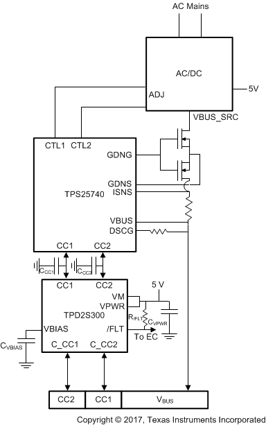 Figure 25. TPD2S300 Typical Application Diagram
8.2.3.1 Design Requirements
In this application example, we use the TPD2S300 to protect a USB Type-C port in a power adaptor application. In this application, the power adaptor needs to supply 20 V, 3 A to the device it is charging. Because 20 V is required, USB-PD needs to be used in this application to achieve this, as USB Type-C alone cannot support higher than 5 V. In order to add USB-PD operation in a power adaptor application, the TPS25740 is used. This device is a USB Type-C and USB PD Source Controller.
With USB-C with 20-V PD being used, a Short-to-VBUS event can occur in the system. This short can affect both the CC and SBU pins. However, in this application, since only USB Type-C and PD charging is required, the SBU pin is not used. Therefore, only CC Short-to-VBUS protection is required to adequately protect the TPS25740 and the system. The CC pins also need IEC61000-4-2 system level ESD protection. Additionally, with this application being a power adaptor, board space is crucial; a small protection device is required. Therefore, with these application requirements, the TPD2S300 is used, a single-chip solution which integrates all the protection requirements needed for the CC pins in this application.
Table 2 shows the TPD2S300 design parameters for this application.
Table 9. Design Parameters
| DESIGN PARAMETER | EXAMPLE VALUE |
|---|---|
| VBUS nominal operating voltage | 20 V |
| Short-to-VBUS tolerance for the CC pins | 24 V |
| VBIAS nominal capacitance | 0.1 µF |
| Dead battery charging | No dead battery mode; source only device |
| TPD2S300 VPWR and VM power source | 5-V source |
| VCONN requirement | VCONN not required |
| Maximum ambient temperature requirement | 85°C |
8.2.3.2 Detailed Design Procedure
8.2.3.2.1 VBIAS Capacitor Selection
This VBIAS capacitor requirements for this application are identical to the Smart-Phone application; please see the VBIAS Capacitor Selection section for more details.
8.2.3.2.2 Dead Battery Operation
This application is source mode only. Therefore, dead battery operation is not required, and RD resistors must not be exposed on the CC lines. However, because when the TPD2S300 is unpowered it exposes its dead battery resistors, when the wall adaptor is not plugged into the wall, it has RDs present on its CC lines. If it is plugged into a laptop at this point, then the laptop senses a connection and output 5-V VBUS. Therefore, the power switch that sources VBUS in the wall adaptor must be able to block this 5-V VBUS from entering the system when it is unplugged from the wall. If this is maintained, there is not any issue. Once, the wall adaptor is plugged into the wall, it turns ON the TPD2S300. This removes the TPD2S300's RD dead battery resistor, and then the laptop stops sourcing VBUS. Once the laptop starts its DRP toggle, it exposes its RD, which causes a connection with the wall adaptor to occur, and the wall adaptor outputs VBUS, and then PD is negotiated like normal.
8.2.3.2.3 CC Line Capacitance
USB PD has a specification for the total amount of capacitance that is required for proper USB PD BMC operation on the CC lines. The specification from section 5.8.6 of the USB PD Specification is given in Table 10.
Table 10. USB PD cReceiver Specification
| NAME | DESCRIPTION | MIN | MAX | UNIT | COMMENT |
|---|---|---|---|---|---|
| cReceiver | CC receiver capacitance | 200 | 600 | pF | The DFP or UFP system shall have capacitance within this range when not transmitting on the line |
Therefore, the capacitance on the CC lines must stay in between 200 pF and 600 pF when USB PD is being used. Therefore, the combination of capacitances added to the system by the TPS25740, the TPD2S300, and any external capacitor must fall within these limits. Table 11 shows the analysis involved in choosing the correct external CC capacitor for this system, and shows that an external CC capacitor is required.
Table 11. CC Line Capacitor Calculation
| CC Capacitance | MIN | MAX | UNIT | COMMENT |
|---|---|---|---|---|
| CC line target capacitance | 200 | 600 | pF | From the USB PD Specification section (cReceiver, section 5.8.6) |
| TPS25740 capacitance | ~0 | 10 | pF | From the TPS25740 Datasheet |
| TPD2S300 capacitance | 30 | 120 | pF | From the Electrical Characteristics table |
| Proposed capacitor GRM033R71E331KA01D | 198 | 462 | pF | CAP, CERM, 330 pF, 25 V, ±10%, X7R, 0201 (For min and max, assume ±40% capacitance change with temperature and voltage derating to be overly conservative) |
| TPS25740 + TPD2S300 + GRM033R71E331KA01D | 228 | 592 | pF | Meets USB PD cReceiver specification |
8.2.3.2.4 FLT Pin Operation
The FLT pin recommendation for this application are identical to the Smart-Phone application; see the FLT Pin Operation section for more details.
8.2.3.2.5 VCONN Operation
In our current application example, VCONN is not required. Therefore, a 3.3-V source or 5-V source can be connected to the VPWR and VM pins of the TPD2S300 to provide adequate resistance in order to support CC analog and USB PD operation over the CC lines. In fact, the CC OVP FETs resistance specifications are set to optimize the FET size and therefore the TPD2S300 size and still allow proper CC analog and USB PD operation. See the Electrical Characteristics table for the specific resistances of the CC OVP FETs.
8.2.3.3 Application Curves
