SLLS683F JULY 2006 – October 2015 TPD3E001
PRODUCTION DATA.
- 1 Features
- 2 Applications
- 3 Description
- 4 Revision History
- 5 Pin Configuration and Functions
- 6 Specifications
- 7 Detailed Description
- 8 Application and Implementation
- 9 Power Supply Recommendations
- 10Layout
- 11Device and Documentation Support
- 12Mechanical, Packaging, and Orderable Information
封装选项
请参考 PDF 数据表获取器件具体的封装图。
机械数据 (封装 | 引脚)
- DRS|6
- DRL|5
- DRY|6
散热焊盘机械数据 (封装 | 引脚)
订购信息
7 Detailed Description
7.1 Overview
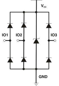
The TPD3E001 is a three-channel Transient Voltage Suppressor (TVS) based Electrostatic Discharge (ESD) protection diode array. The TPD3E001 is rated to dissipate ESD strikes at the maximum level specified in the IEC 61000-4-2 international standard (Level 4). This device has a 1.5-pF IO capacitance per channel, making it ideal for use in high-speed data IO interfaces. The ultra low leakage current (< 1 nA maximum) is suitable for precision analog measurements in applications like glucose meters and heart rate monitors. The wide voltage range on VCC (up to 5.5V) gives this device the flexibility to be used in a wide variety applications. Having 3-channels of ESD protection makes this device particularly well suited to protect a micro-AB USB connector, which has three signal lines to be protected (D+, D-, ID). The VBUS pin can also be protected by connecting it to VCC on TPD3E001. Therefore, TPD3E001 is a one-chip solution to provide Level 4 IEC 61000-4-2 ESD protection on every pin of the micro-AB USB connector.
7.2 Functional Block Diagram

7.3 Feature Description
TPD3E001 is a uni-directional ESD protection device with low capacitance. The device is constructed with a central ESD clamp that features two hiding diodes per line to reduce the capacitive loading. This central ESD clamp is also connected to VCC to provide protection for the VCC line. Each IO line is rated to dissipate ESD strikes at the maximum level specified in the IEC 61000-4-2 level 4 international standard. The TPD3E001's low loading capacitance makes it ideal for protection high-speed signal terminals.
7.4 Device Functional Modes
TPD3E001 is a passive-integrated circuit that activates whenever voltages above VBR or below the lower diodes Vforward (–0.6V) are present upon the circuit being protected. During ESD events, voltages as high as ±15 kV can be directed to ground and VCC via the internal diode network. Once the voltages on the protected lines fall below the trigger voltage of the TPD3E001 (usually within 10's of nano-seconds) the device reverts back to a high-impedance state.