ZHCSD89A October   2014  – January 2015 TPD3S014 , TPD3S044

PRODUCTION DATA.  

  1. 特性
  2. 应用
  3. 说明
  4. 简化电路原理图
  5. 修订历史记录
  6. Device Comparison
  7. Pin Configuration and Functions
  8. Specifications
    1. 8.1 Absolute Maximum Ratings
    2. 8.2 ESD Ratings
    3. 8.3 Recommended Operating Conditions
    4. 8.4 Thermal Information
    5. 8.5 Electrical Characteristics: TJ = TA = 25°C
    6. 8.6 Electrical Characteristics: -40°C ≤ TJ ≤ 125°C
    7. 8.7 Typical Characteristics
  9. Detailed Description
    1. 9.1 Overview
    2. 9.2 Functional Block Diagram
    3. 9.3 Feature Description
      1. 9.3.1 Undervoltage Lockout (UVLO)
      2. 9.3.2 Enable
      3. 9.3.3 Internal Charge Pump
      4. 9.3.4 Current Limit
      5. 9.3.5 Output Discharge
      6. 9.3.6 Input and Output Capacitance
      7. 9.3.7 Power Dissipation and Junction Temperature
    4. 9.4 Device Functional Modes
      1. 9.4.1 Operation with VIN < 4 V (Minimum VIN)
      2. 9.4.2 Operation With EN Control
      3. 9.4.3 Operation of Level 4 IEC61000-4-2 ESD Protection
  10. 10Application and Implementation
    1. 10.1 Application Information
    2. 10.2 Typical Application
      1. 10.2.1 USB2.0 Application
        1. 10.2.1.1 Design Requirements
        2. 10.2.1.2 Detailed Design Procedure
        3. 10.2.1.3 Application Curves
      2. 10.2.2 USB3.0 Application
        1. 10.2.2.1 Design Requirements
        2. 10.2.2.2 Detailed Design Procedure
        3. 10.2.2.3 Application Curves
  11. 11Power Supply Recommendations
  12. 12Layout
    1. 12.1 Layout Guidelines
    2. 12.2 Layout Examples
  13. 13器件和文档支持
    1. 13.1 相关链接
    2. 13.2 商标
    3. 13.3 静电放电警告
    4. 13.4 术语表
  14. 14机械封装和可订购信息

封装选项

机械数据 (封装 | 引脚)
散热焊盘机械数据 (封装 | 引脚)
订购信息

7 Pin Configuration and Functions

DBV PACKAGE
SOT23 6-PIN
(2.9 mm × 2.8 mm × 1.45 mm)
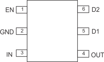
TPD3S014 TPD3S044 po_slvscp4.gif

Pin Functions

PIN DESCRIPTION
NAME NO.
D1 5 USB data+ or USB data–
D2 6
EN 1 Enable input, logic high turns on power switch
GND 2 Ground
IN 3 Input voltage and power-switch drain; Connect a 0.1 µF or greater ceramic capacitor from IN to GND close to the IC
OUT 4 Power-switch output, connect to load