ZHCSAL0D March 2016 – August 2020 TPD3S716-Q1
PRODUCTION DATA
- 1 特性
- 2 应用
- 3 说明
- 4 Revision History
- 5 Pin Configuration and Functions
- 6 Specifications
- 7 Parameter Measurement Information
-
8 Detailed Description
- 8.1 Overview
- 8.2 Functional Block Diagram
- 8.3
Feature Description
- 8.3.1 AEC-Q100 Qualified
- 8.3.2 Short-to-Battery and Short-to-Ground Protection on VBUS_CON
- 8.3.3 Short-to-Battery and Short-to-VBUS Protection on VD+, VD–
- 8.3.4 ESD Protection on VBUS_CON, VD+, VD–
- 8.3.5 Low RON nFET VBUS Switch
- 8.3.6 High Speed Data Switches
- 8.3.7 Adjustable Hiccup Current Limit up to 2.4-A
- 8.3.8 Fast Over-Voltage Response Time
- 8.3.9 Independent VBUS and Data Enable Pins for Configuring both Host and Client/OTG Mode
- 8.3.10 Fault Output Signal
- 8.3.11 Thermal Shutdown Feature
- 8.3.12 16-Pin SSOP Package
- 8.3.13 Reverse Current Detection
- 8.4 Device Functional Modes
- 9 Application and Implementation
- 10Power Supply Recommendations
- 11Layout
- 12Device and Documentation Support
- 13Mechanical, Packaging, and Orderable Information
11.3 Layout Optimized for Thermal Performance
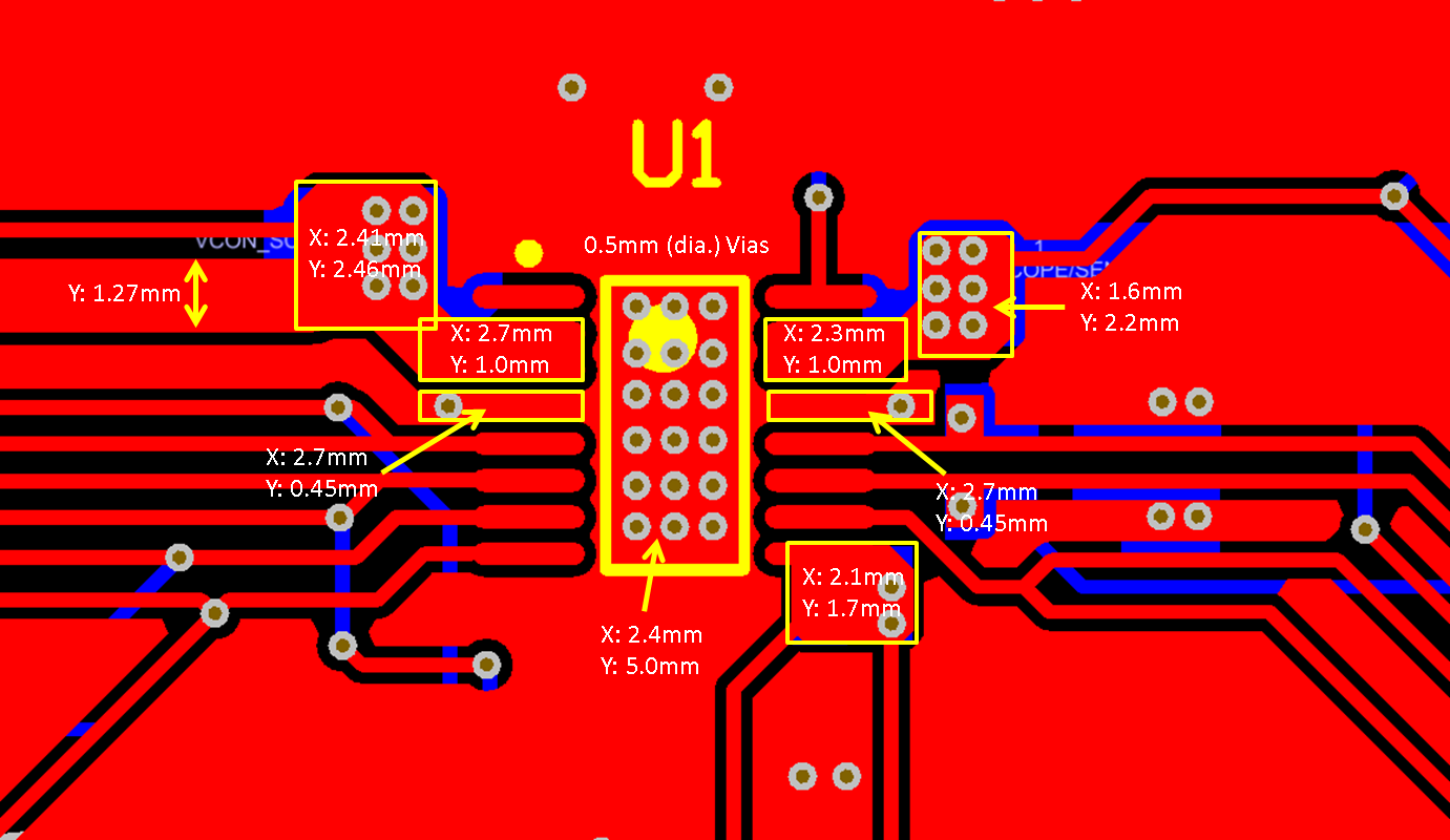
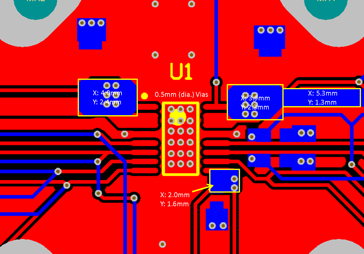
Figure 11-2 and Figure 11-3 show images from a real PCB design optimized for the best thermal performance for TPD3S716-Q1. This PCB layout has 6 layers (2 signal and 4 plane layers). The 2 signal layers are the outer layers of the PCB and constructed with 2-oz copper, and the 4 internal plane layers are constructed with 1-oz copper. Using this PCB layout yielded an RθJA(CUSTOM) = 57 (°C/W). The images contain rough dimensions of the copper traces and pours used around the device. One key strategy to optimize thermal performance of the device is to maximize the area of the copper pours and traces used to route the device power, GND, and signal pins when possible. Another key strategy is to maximize the copper weight of the PCB metal layers. This example demonstrates that excellent thermal performance can be achieved with TPD3S716-Q1 with the proper PCB layout.
 Figure 11-2 Thermally Optimized PCB Layout Top Layer
 Figure 11-3 Thermally Optimized PCB Layout Bottom Layer