ZHCSB23F March   2013  – September 2017 TPD4E001-Q1

PRODUCTION DATA.  

  1. 特性
  2. 应用
  3. 说明
  4. 修订历史记录
  5. Pin Configuration and Functions
  6. Specifications
    1. 6.1 Absolute Maximum Ratings
    2. 6.2 ESD Ratings—AEC Specification
    3. 6.3 ESD Ratings—IEC Specification
    4. 6.4 ESD Ratings—ISO Specification
    5. 6.5 Recommended Operating Conditions
    6. 6.6 Thermal Information
    7. 6.7 Electrical Characteristics
    8. 6.8 Typical Characteristics
  7. Detailed Description
    1. 7.1 Overview
    2. 7.2 Functional Block Diagram
    3. 7.3 Feature Description
      1. 7.3.1 AEC-Q100 Qualified
      2. 7.3.2 IEC 61000-4-2 Level 4 ESD Protection
      3. 7.3.3 IEC 61000-4-5 Surge Protection
      4. 7.3.4 Low 1.5-pF Input Capacitance
      5. 7.3.5 Low 10-nA (Maximum) Leakage Current
      6. 7.3.6 0.9-V to 5.5-V Supply Voltage Range
    4. 7.4 Device Functional Modes
  8. Application and Implementation
    1. 8.1 Application Information
    2. 8.2 Typical Application
      1. 8.2.1 Design Requirements
      2. 8.2.2 Detailed Design Procedure
        1. 8.2.2.1 Signal Range on IO1 Through IO4
        2. 8.2.2.2 Voltage Range on VCC
        3. 8.2.2.3 Bandwidth on IO1 Through IO4
      3. 8.2.3 Application Curve
  9. Power Supply Recommendations
  10. 10Layout
    1. 10.1 Layout Guidelines
    2. 10.2 Layout Example
  11. 11器件和文档支持
    1. 11.1 文档支持
      1. 11.1.1 相关文档
    2. 11.2 接收文档更新通知
    3. 11.3 社区资源
    4. 11.4 商标
    5. 11.5 静电放电警告
    6. 11.6 Glossary
  12. 12机械、封装和可订购信息

封装选项

机械数据 (封装 | 引脚)
散热焊盘机械数据 (封装 | 引脚)
订购信息

Pin Configuration and Functions

DBV Package
6-Pin SOT-23
Top View
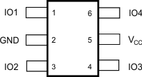
TPD4E001-Q1 po_SLLSEG0.gif

Pin Functions

PIN TYPE DESCRIPTION
NAME NO.
GND 2 GND Ground
IO1 1 I/O ESD-protected channel
IO2 3
IO3 4
IO4 6
VCC 5 I Power-supply input. Bypass VCC to GND with a 0.1-μF ceramic capacitor