ZHCSEN2A November 2015 – February 2016 TPD4E02B04
PRODUCTION DATA.
- 1 特性
- 2 应用
- 3 说明
- 4 修订历史记录
- 5 Pin Configuration and Functions
- 6 Specifications
-
7 Detailed Description
- 7.1 Overview
- 7.2 Functional Block Diagram
- 7.3
Feature Description
- 7.3.1 IEC 61000-4-2 ESD Protection
- 7.3.2 IEC 61000-4-4 EFT Protection
- 7.3.3 IEC 61000-4-5 Surge Protection
- 7.3.4 IO Capacitance
- 7.3.5 DC Breakdown Voltage
- 7.3.6 Ultra Low Leakage Current
- 7.3.7 Low ESD Clamping Voltage
- 7.3.8 Supports High Speed Interfaces
- 7.3.9 Industrial Temperature Range
- 7.3.10 Easy Flow-Through Routing Package
- 7.4 Device Functional Modes
- 8 Application and Implementation
- 9 Power Supply Recommendations
- 10Layout
- 11器件和文档支持
- 12机械、封装和可订购信息
10 Layout
10.1 Layout Guidelines
- The optimum placement is as close to the connector as possible.
- EMI during an ESD event can couple from the trace being struck to other nearby unprotected traces, resulting in early system failures.
- The PCB designer needs to minimize the possibility of EMI coupling by keeping any unprotected traces away from the protected traces which are between the TVS and the connector.
- Route the protected traces as straight as possible.
- Eliminate any sharp corners on the protected traces between the TVS and the connector by using rounded corners with the largest radii possible.
- Electric fields tend to build up on corners, increasing EMI coupling.
10.2 Layout Examples
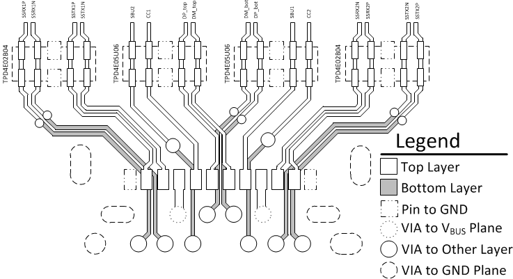
 Figure 24. USB Type-C Mid-Mount, Hybrid Connector with One-Sided ESD Layout
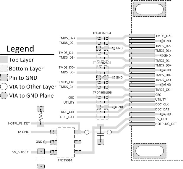
 Figure 25. HDMI2.0 Type-A Transmitter Port Layout