ZHCSAT4D December 2012 – April 2017 TPD4E1U06
PRODUCTION DATA.
8 Application and Implementation
NOTE
Information in the following applications sections is not part of the TI component specification, and TI does not warrant its accuracy or completeness. TI’s customers are responsible for determining suitability of components for their purposes. Customers should validate and test their design implementation to confirm system functionality.
8.1 Application Information
The TPD4E1U06 is a TVS diode array which is typically used to provide a path to ground for dissipating ESD events on hi-speed signal lines between a human interface connector and a system. As the current from ESD passes through the TVS, only a small voltage drop is present across the diode. This is the voltage presented to the protected IC. The low RDYN of the triggered TVS holds this voltage, VCLAMP, to a safe level for the protected IC.
8.2 Typical Application
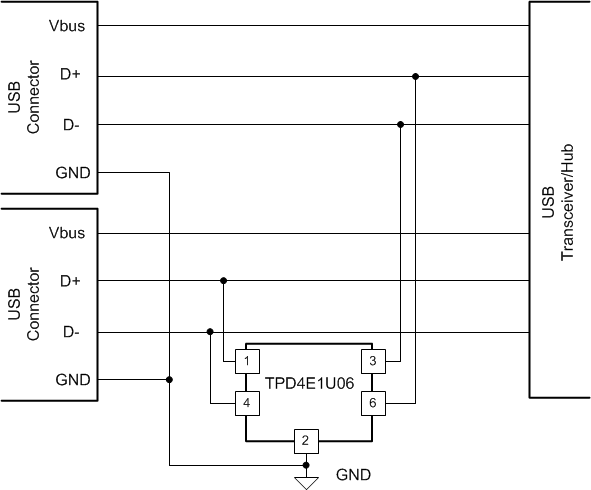
For this design example, one TPD4E1U06 device is being used in a dual USB 2.0 application. This provides a complete port protection scheme.
 Figure 10. Dual USB 2.0 Application
8.2.1 Design Requirements
Given the USB 2.0 application, the parameters in Table 1 are known.
Table 1. Design Parameters
| DESIGN PARAMETER | VALUE |
|---|---|
| Signal range on pins 1, 3, 4, or 6 | 0 V to 5 V |
| Operating frequency | 240 MHz |
8.2.2 Detailed Design Procedure
8.2.2.1 Signal Range on Pins 1, 3, 4, or 6
The TPD4E1U06 has 4 identical protection channels for signal lines. The symmetry of the device provides flexibility when selecting which of the 4 I/O channels protect which signal lines. Any I/O supports a signal range of 0 to 5.5 V.
8.2.2.2 Operating Frequency
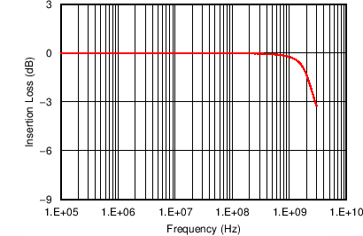
The TPD4E1U06 has a capacitance of 0.8 pF (typical), supporting USB 2.0 data rates.
8.2.3 Application Curve
 Figure 11. Insertion Loss Graph