SLVS817G May 2008 – June 2015 TPD4S009 , TPD4S010
PRODUCTION DATA.
- 1 Features
- 2 Applications
- 3 Description
- 4 Revision History
- 5 Pin Configuration and Functions
- 6 Specifications
-
7 Detailed Description
- 7.1 Overview
- 7.2 Functional Block Diagram
- 7.3
Feature Description
- 7.3.1 ±8-kV IEC61000-4-2 Level 4 Contact ESD Protection
- 7.3.2 IEC61000-4-5 Surge Protection
- 7.3.3 I/O Capacitance
- 7.3.4 Low Leakage Current
- 7.3.5 Supports High-Speed Differential Data Rates
- 7.3.6 Ultra-low Matching Capacitance Between Differential Signal Pairs
- 7.3.7 Ioff Feature for the TPD4S009
- 7.3.8 Industrial Temperature Range
- 7.3.9 Easy Flow-Through Routing
- 7.4 Device Functional Modes
- 8 Application and Implementation
- 9 Power Supply Recommendations
- 10Layout
- 11Device and Documentation Support
- 12Mechanical, Packaging, and Orderable Information
10 Layout
10.1 Layout Guidelines
- The optimum placement is as close to the connector as possible.
- EMI during an ESD event can couple from the trace being struck to other nearby unprotected traces, resulting in early system failures.
- The PCB designer needs to minimize the possibility of EMI coupling by keeping any unprotected traces away from the protected traces which are between the TVS and the connector.
- Route the protected traces as straight as possible.
- Eliminate any sharp corners on the protected traces between the TVS and the connector by using rounded corners with the largest radii possible.
- Electric fields tend to build up on corners, increasing EMI coupling.
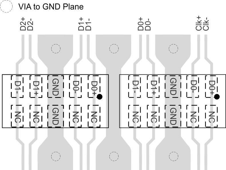
10.2 Layout Example
This is a layout example for TPD4S010 being used to protect HDMI TMDS Lines.
 Figure 11. TPD4S010 Layout