SLVS817G May   2008  – June 2015 TPD4S009 , TPD4S010

PRODUCTION DATA.  

  1. Features
  2. Applications
  3. Description
  4. Revision History
  5. Pin Configuration and Functions
  6. Specifications
    1. 6.1 Absolute Maximum Ratings
    2. 6.2 ESD Ratings
    3. 6.3 Recommended Operating Conditions
    4. 6.4 Thermal Information
    5. 6.5 Electrical Characteristics
    6. 6.6 Typical Characteristics
  7. Detailed Description
    1. 7.1 Overview
    2. 7.2 Functional Block Diagram
    3. 7.3 Feature Description
      1. 7.3.1 ±8-kV IEC61000-4-2 Level 4 Contact ESD Protection
      2. 7.3.2 IEC61000-4-5 Surge Protection
      3. 7.3.3 I/O Capacitance
      4. 7.3.4 Low Leakage Current
      5. 7.3.5 Supports High-Speed Differential Data Rates
      6. 7.3.6 Ultra-low Matching Capacitance Between Differential Signal Pairs
      7. 7.3.7 Ioff Feature for the TPD4S009
      8. 7.3.8 Industrial Temperature Range
      9. 7.3.9 Easy Flow-Through Routing
    4. 7.4 Device Functional Modes
  8. Application and Implementation
    1. 8.1 Application Information
    2. 8.2 Typical Application
      1. 8.2.1 Design Requirements
      2. 8.2.2 Detailed Design Procedure
        1. 8.2.2.1 Signal Range on Pin 1, 2, 4, or 5
        2. 8.2.2.2 Bandwidth on Pin 1, 2, 4, or 5
      3. 8.2.3 Application Curves
  9. Power Supply Recommendations
  10. 10Layout
    1. 10.1 Layout Guidelines
    2. 10.2 Layout Example
  11. 11Device and Documentation Support
    1. 11.1 Documentation Support
      1. 11.1.1 Related Documentation
    2. 11.2 Trademarks
    3. 11.3 Electrostatic Discharge Caution
    4. 11.4 Glossary
  12. 12Mechanical, Packaging, and Orderable Information

封装选项

机械数据 (封装 | 引脚)
散热焊盘机械数据 (封装 | 引脚)
订购信息

5 Pin Configuration and Functions

TPD4S009 DBV OR DCK PACKAGE
6-PIN SOT
TOP VIEW
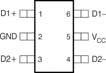
TPD4S009 TPD4S010 po_01_lvs817.gif
TPD4S009 DGS PACKAGE
10-PIN VSSOP
TOP VIEW
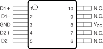
TPD4S009 TPD4S010 po_02_lvs817.gif
TPD4S010 DQA PACKAGE
10-PIN USON
TOP VIEW
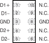
TPD4S009 TPD4S010 po_03_lvs817.gif
TPD4S009 DRY PACKAGE
6-PIN USON
TOP VIEW
TPD4S009 TPD4S010 po_04_lvs817.gif

Pin Functions

PIN I/O DESCRIPTION
NAME SOT or USON VSSOP USON
D1+ 1 1 1 ESD port High-speed ESD clamp provides ESD protection to the high-speed differential data lines.
D1– 6 2 2
D2+ 3 4 4
D2– 4 5 5
GND 2 3 3, 8 GND Ground
N.C. 6, 7, 9, 10 6, 7, 9, 10 Not internally connected
VCC 5 8 Power Supply