ZHCSAD1D October 2012 – June 2017 TPD5S115
PRODUCTION DATA.
- 1 特性
- 2 应用
- 3 说明
- 4 修订历史记录
- 5 Pin Configuration and Functions
-
6 Specifications
- 6.1 Absolute Maximum Ratings
- 6.2 ESD Ratings
- 6.3 Recommended Operating Conditions
- 6.4 Thermal Information
- 6.5 Electrical Characteristics
- 6.6 Electrical Characteristics - I/O Capacitances
- 6.7 Switching Characteristics - VCCA = 1.2 V
- 6.8 Switching Characteristics - VCCA = 1.5 V
- 6.9 Switching Characteristics - VCCA = 1.8 V
- 6.10 Switching Characteristics - VCCA = 2.5 V
- 6.11 Switching Characteristics - VCCA = 3.3 V
- 6.12 Typical Characteristics
- 7 Detailed Description
- 8 Application and Implementation
- 9 Power Supply Recommendations
- 10Layout
- 11器件和文档支持
- 12机械、封装和可订购信息
10 Layout
10.1 Layout Guidelines
For proper operation, follow these layout and design guidelines:
- Place the TPD5S115 as close to the connector as possible. This allows it to remove the energy associated with ESD strike before it reaches the internal circuitry of the system board.
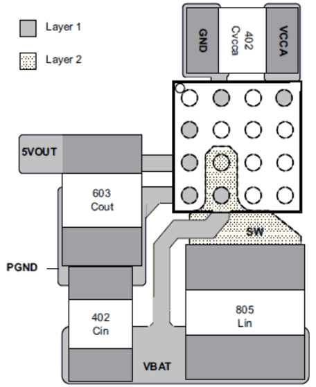
- Place power line capacitors and inductors close to the pins with wide traces to allow enough current to flow through with less trace parasitics. Ensure that there is enough metallization for the GND pad. A sufficient current path enables safe discharge of all the energy associated with the ESD strike.
10.2 Layout Example
 Figure 17. Board Layout With DC-DC Components (Top View)