ZHCSAD1D October 2012 – June 2017 TPD5S115
PRODUCTION DATA.
- 1 特性
- 2 应用
- 3 说明
- 4 修订历史记录
- 5 Pin Configuration and Functions
-
6 Specifications
- 6.1 Absolute Maximum Ratings
- 6.2 ESD Ratings
- 6.3 Recommended Operating Conditions
- 6.4 Thermal Information
- 6.5 Electrical Characteristics
- 6.6 Electrical Characteristics - I/O Capacitances
- 6.7 Switching Characteristics - VCCA = 1.2 V
- 6.8 Switching Characteristics - VCCA = 1.5 V
- 6.9 Switching Characteristics - VCCA = 1.8 V
- 6.10 Switching Characteristics - VCCA = 2.5 V
- 6.11 Switching Characteristics - VCCA = 3.3 V
- 6.12 Typical Characteristics
- 7 Detailed Description
- 8 Application and Implementation
- 9 Power Supply Recommendations
- 10Layout
- 11器件和文档支持
- 12机械、封装和可订购信息
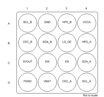
5 Pin Configuration and Functions
Pin Functions
| PIN | TYPE(1) | DESCRIPTION | |
|---|---|---|---|
| NAME | NO. | ||
| 5VOUT | C1 | O | DC-DC output. The 5-V power pin can supply a 55-mA regulated current to the HDMI receiver. A separate DC-DC converter control pin (EN) disables the DC-DC converter when operating at low-power mode |
| CEC_A | D3 | I/O | LS system side CEC bus I/O. This pin is bidirectional and referenced to VCCA |
| CEC_B | B1 | I/O | LS HDMI connector side CEC bus I/O. This pin is bidirectional and referenced to the 3.3-V internal supply |
| EN | C3 | C | DC-DC enable. Enables the DC-DC converter and HPD circuitry when EN is HIGH. The EN is referenced based off VCCA |
| GND | A2 | G | Device ground |
| HPD_A | B4 | O | System side output for the hot plug detect. This pin is unidirectional and is referenced to VCCA |
| HPD_B | A3 | I | HDMI side input for the hot plug detect. This pin is unidirectional and is referenced to 5VOUT |
| LS_OE | B3 | C | Level shifter enable. This pin is referenced to VCCA. Enables level shifters and LDO when EN is HIGH and LS_OE is HIGH |
| PGND | D1 | G | DC-DC converter ground. These pins are isolated from the GND pins. This pin should be tied to system GND |
| SCL_A, SDA_A | D4, C4 | I/O | LS system side input and output for I2C Bus. These pins are bidirectional and referenced to VCCA |
| SCL_B, SDA_B | A1, B2 | I/O | LS HDMI side connector side input and output for I2C Bus. These pins are bidirectional and referenced to 5VOUT |
| SW | C2 | I | Switch input. This pin is the inductor input for the DC-DC converter |
| VBAT | D2 | P | Battery supply. This voltage is typically 2.3 V to 5.5 V |
| VCCA | A4 | P | System side supply. This voltage is typically 1.2 V to 3.3 V from the core microcontroller |
(1) C = Control, G = Ground, I = Input, O = Output, P = Power
