ZHCSAD1D October 2012 – June 2017 TPD5S115
PRODUCTION DATA.
- 1 特性
- 2 应用
- 3 说明
- 4 修订历史记录
- 5 Pin Configuration and Functions
-
6 Specifications
- 6.1 Absolute Maximum Ratings
- 6.2 ESD Ratings
- 6.3 Recommended Operating Conditions
- 6.4 Thermal Information
- 6.5 Electrical Characteristics
- 6.6 Electrical Characteristics - I/O Capacitances
- 6.7 Switching Characteristics - VCCA = 1.2 V
- 6.8 Switching Characteristics - VCCA = 1.5 V
- 6.9 Switching Characteristics - VCCA = 1.8 V
- 6.10 Switching Characteristics - VCCA = 2.5 V
- 6.11 Switching Characteristics - VCCA = 3.3 V
- 6.12 Typical Characteristics
- 7 Detailed Description
- 8 Application and Implementation
- 9 Power Supply Recommendations
- 10Layout
- 11器件和文档支持
- 12机械、封装和可订购信息
6 Specifications
6.1 Absolute Maximum Ratings
over operating free-air temperature range (unless otherwise noted)(1)| MIN | MAX | UNIT | ||
|---|---|---|---|---|
| Supply voltage | VCCA | 4 | V | |
| VBAT | –0.3 | 6 | V | |
| Input voltage, VI(2) | SCL_A, SDA_A, CEC_A | –0.3 | 4 | V |
| SCL_B, SDA_B, CEC_B, HPD_B | –0.3 | 6 | ||
| EN, LS_OE | –0.3 | 4 | ||
| Voltage applied to any output in the high-impedance or power‑off state, VO(2) | SCL_A, SDA_A, CEC_A | –0.3 | 4 | V |
| SCL_B, SDA_B, CEC_B | –0.3 | 6 | ||
| Voltage applied to any output in the high or low state, VO(2) | SCL_A, SDA_A, CEC_A | –0.3 | VCCA + 0.3 | V |
| SCL_B, SDA_B, CEC_B | –0.3 | 5VOUT + 0.3 | ||
| Input clamp current (IV < 0) | –50 | mA | ||
| Output clamp current (VO < 0) | –50 | mA | ||
| Continuous current through 5VOUT, or GND | ±100 | mA | ||
| Storage temperature, Tstg | –65 | 150 | °C | |
(1) Stresses beyond those listed under Absolute Maximum Ratings may cause permanent damage to the device. These are stress ratings only, which do not imply functional operation of the device at these or any other conditions beyond those indicated under Recommended Operating Conditions. Exposure to absolute-maximum-rated conditions for extended periods may affect device reliability.
(2) The input and output voltage ratings may be exceeded if the input and output clamp-current ratings are observed.
6.2 ESD Ratings
| VALUE | UNIT | ||||
|---|---|---|---|---|---|
| V(ESD) | Electrostatic discharge | Human-body model (HBM), per ANSI/ESDA/JEDEC JS-001(1) | All pins except pins 4A, B3, C3, C4, D3, and D4 | 500 | V |
| Pins 4A, B3, C3, C4, D3, and D4 | 2000 | ||||
| Charged-device model (CDM), per JEDEC specification JESD22-C101(2) | 1000 | ||||
| IEC 61000-4-2 Contact Discharge | Pins A1, A3, B1, B2, and C1 | ±14000 | |||
| IEC 61000-4-2 Air-gap Discharge | Pins A1, A3, B1, B2, and C1 | ±16000 | |||
(1) JEDEC document JEP155 states that 500-V HBM allows safe manufacturing with a standard ESD control process.
(2) JEDEC document JEP157 states that 250-V CDM allows safe manufacturing with a standard ESD control process.
6.3 Recommended Operating Conditions
over operating free-air temperature range (unless otherwise noted)| MIN | NOM | MAX | UNIT | ||||
|---|---|---|---|---|---|---|---|
| VCCA | Supply voltage, VCCA | 1.2 | 3.6 | V | |||
| VBAT | Supply voltage, VBAT | 2.3 | 5.5 | V | |||
| VIH | High-level input voltage | VCCA = 1.2 V to 3.6 V | SCL_A, SDA_A | 0.7 × VCCA | VCCA | V | |
| CEC_A | 0.7 × VCCA | VCCA | |||||
| EN, LS_OE | 1 | VCCA | |||||
| 5VOUT = 5 V | SCL_B, SDA_B | 0.7 × 5VOUT | 5VOUT | ||||
| CEC_B | 0.7 × 3.3 V (internal)(1) | 3.3 V (internal)(1) | |||||
| HPD_B | 2 | ||||||
| VIL | Low-Level input voltage | VCCA = 1.2 V to 3.6 V | SCL_A, SDA_A | –0.5 | 0.082 × VCCA | V | |
| CEC_A | –0.5 | 0.082 × VCCA | |||||
| EN, LS_OE | –0.5 | 0.4 | |||||
| 5VOUT = 5 V | SCL_B, SDA_B | –0.5 | 0.3 × 5VOUT | ||||
| CEC_B | –0.5 | 0.3 × 3.3 (internal)(1) | |||||
| HPD_B | 0 | 0.8 | |||||
| VILC | Low-level input voltage | –0.5 | 0.065 × VCCA | V | |||
| VOL – VILC | Delta between VOL and VILC (VIO = 2.5 V) | 0.1 × VCCA | V | ||||
| TA | Operating free-air temperature | –40 | 85 | °C | |||
(1) 3.3 V (internal) is an internally generated voltage node for the CEC_B output buffer supply reference. An LDO generates this 3.3 V from 5VOUT when LS_OE and EN are HIGH.
6.4 Thermal Information
| THERMAL METRIC(1) | TPD5S115 | UNIT | |
|---|---|---|---|
| YFF (DSBGA) | |||
| 16 PINS | |||
| RθJA | Junction-to-ambient thermal resistance | 78.2 | °C/W |
| RθJC(top) | Junction-to-case (top) thermal resistance | 0.6 | °C/W |
| RθJB | Junction-to-board thermal resistance | 13.2 | °C/W |
| ψJT | Junction-to-top characterization parameter | 2.5 | °C/W |
| ψJB | Junction-to-board characterization parameter | 13 | °C/W |
(1) For more information about traditional and new thermal metrics, see the Semiconductor and IC Package Thermal Metrics application report.
6.5 Electrical Characteristics
TA = –40°C to 85°C (unless otherwise noted)| PARAMETER | TEST CONDITIONS | MIN | TYP | MAX | UNIT | ||
|---|---|---|---|---|---|---|---|
| VOHA | IOH = –10 µA, VI = VIH, VCCA = 1.2 V to 3.6 V | VCCA × 0.8 | V | ||||
| VOLA | IOL = 10 µA, VI = VIL, VCCA = 1.2 V to 3.6 V | VCCA × 0.16 | V | ||||
| VOHB | IOH = –10 µA, VI = VIH | V | |||||
| VOLB | IOL = 3 mA, VI = VIL | 0.4 | V | ||||
| RPU | Internal pullup | SCL_A, SDA_A | Pullup connected to VCCA rail | 10 | kΩ | ||
| SCL_B, SDA_B | Pullup connected to 5-V rail | 1.75 | |||||
| IPULLUPAC | Transient boosted pullup current (rise-time accelerator) |
SCL_B, SDA_B | Pullup connected to 5-V rail | 15 | mA | ||
| IOFF | Leakage current | A port | VCCA = 0 V, VI or VO = 0 to 3.6 V, VCCA = 0 V | ±5 | µA | ||
| B port | 5VOUT = 0 V, VI or VO = 0 to 5.5 V, VCCA = 0 V to 3.6 V | ±5 | |||||
| IOZ | A port | VO = VCCO or GND, VCCA = 1.2 V to 3.6 V | ±5 | ||||
| B port | VI = VCCI or GND, VCCA = 1.2 V to 3.6 V | ±5 | |||||
| CL | Bus load capacitance | A port | 15 | pF | |||
| B port | 750 | ||||||
| SUPPLY CURRENT | |||||||
| ICCA | VCCA supply current | Standby | I/Os = HIGH | 2 | µA | ||
| Active | I/Os = HIGH | 15 | µA | ||||
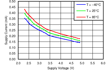
| ICCB | VBAT supply current | Standby | EN = LOW, LS_OE = LOW | 0.5 | µA | ||
| DC-DC and HPD active |
EN = HIGH, LS_OE = LOW | 30 | 50 | µA | |||
| DC-DC, HPD, DDC, CEC Active | EN = HIGH, LS_OE = LOW, I/Os = HIGH | 225 | 300 | µA | |||
| DC-DC CONVERTER | |||||||
| VBAT | Input voltage | 2.3 | 5.5 | V | |||
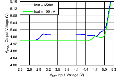
| VOUT | Total DC output voltage(1) | 4.9 | 5 | 5.13 | V | ||
| TOVA | Total output voltage accuracy(2) | 4.8 | 5 | 5.3 | V | ||
| VIO_Ripple | Output voltage ripple, loaded | IO = 65 mA | 50.6 | mVPP | |||
| IO = 150 mA | 16 | ||||||
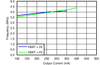
| fCLK | Internal operating frequency | VBAT = 2.3 V to 5.5 V | 3.5 | MHz | |||
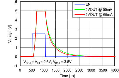
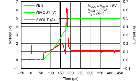
| tSTART | Start-up time | From EN input to 5-V power output 90% point | 187 | µs | |||
| IO | Output current | VBAT = 2.3 V to 5.5 V | 55 | mA | |||
| Reverse leakage current, VO | EN = LOW, VO = 5.5 V | 2.5 | µA | ||||
| Leakage current from battery to VO | EN = LOW | 5 | µA | ||||
| VBATUV | Undervoltage lockout threshold | Falling | 2 | V | |||
| Rising | 2.1 | V | |||||
| Line transient response | VBAT = 3.4 V, IO = 20 mA to 65 mA, A 217 Hz, 600 mVPP square wave pulse |
17.1 | mVpk | ||||
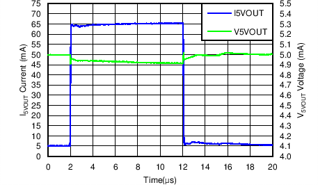
| Load transient response | VBAT = 3.4 V, IO = 5 mA to 65 mA, 10-µs pulse, tRISE = tFALL = 0.1 µs |
63.5 | mVpk | ||||
| IINRUSH | Inrush current, average over tSTART | VBAT = 2.3 V to 5.5 V, IOUT = 65 mA | 168 | mA | |||
| ISC | Short-circuit current limit from output | 90 | mA | ||||
| VOLTAGE LEVEL SHIFTER CEC LINE (x_A & x_B PORTS) | |||||||
| VOHA | IOH = –10 µA, VI = VIH, VCCA = 1.2 V to 3.6 V | VCCA × 0.8 | V | ||||
| VOLA | IOL = 10 µA, VI = VIL, VCCA = 1.2 V to 3.6 V | VCCA × 0.16 | V | ||||
| VOHB | IOH = –20 µA, VI = VIH | VCCA × 0.8 | V | ||||
| VOLB | IOL = 3 mA, VI = VIL | 0.4 | V | ||||
| RPU | Internal pullup | CEC_A | Pullup connected to VCCA rail | 10 | kΩ | ||
| CEC_B | Pullup connected to 3.3 V rail | 22 | 26 | 30 | |||
| RPD | Internal pulldown | CEC_B | Pullup connected to GND | 14 | MΩ | ||
| IOFF | A port | VCCA = 0 V, VI or VO = 0 to 3.6 V, VCCA = 0 V | ±5 | µA | |||
| B port | 5VOUT = 0 V, VI or VO = 0 to 5.5 V, VCCA = 0 V to 3.6 V | ±1.8 | |||||
| IOZ | A port | VO = VCCO or GND, VCCA = 1.2 V to 3.6 V | ±5 | ||||
| B port | VI = VCCI or GND, VCCA = 1.2 V to 3.6 V | ±5 | |||||
| VOLTAGE LEVEL SHIFTER - HPD LINE (X_A & x_B) | |||||||
| VOHA | IOH = –3 mA, VI = VIH, VCCA = 1.2 V to 3.6 V | VCCA × 0.7 | V | ||||
| VOLA | IOL = 3 mA, VI = VIL, VCCA = 1.2 V to 3.6 V | 0.4 | V | ||||
| RPD | Internal pulldown | HPD_B | Pullup connected to GND | 100 | kΩ | ||
| IOZ | A port | VI = VCCI or GND, VCCA = 3.6 V | ±5 | µA | |||
| LS_OE, EN | |||||||
| II | VI = VCCA or GND, VCCA = 1.2 V to 3.6 V | ±12 | |||||
(1) Includes voltage references, DC load and line regulations, process and temperature.
(2) Includes voltage references, DC load and line regulations, transient load and line regulations, ripple, process, and temperature.
6.6 Electrical Characteristics – I/O Capacitances
over operating free-air temperature range (unless otherwise noted)| PARAMETER | TEST CONDITIONS | MIN | TYP | MAX | UNIT | ||
|---|---|---|---|---|---|---|---|
| Capacitance | EN, LS_OE | VBIAS = 1.8 V, f = 1 MHz, 30-mVPP AC signal |
VCCA = 3.6 V, VBAT = 5 V | 7.1 | 9.5 | pF | |
| SCL_A, SDA_A, CEC_A | VCCA = 3.6 V, VBAT = 5 V, EN = LOW | 7 | pF | ||||
| HPD_A, HPD_B | VCCA = 3.6 V, VBAT = 5 V, EN = LOW | 4 | pF | ||||
| SCL_B, SDA_B | VBIAS = 2.5 V, f = 100 kHz, 3.5-VPP AC signal |
VCCA = 3.6 V, VBAT = 5 V, EN = LOW, LS_OE = HIGH | 10 | pF | |||
| CEC_B | VBIAS = 1.65 V, f = 100 kHz, 2.5-VPP AC signal |
VCCA = 3.6 V, VBAT = 5 V, EN = LOW, LS_OE = HIGH | 7 | pF | |||
| CEC_B | VCCA = 0 V, 5V_IN = 0 V | 7 | pF | ||||
6.7 Switching Characteristics – VCCA = 1.2 V
over operating free-air temperature range (unless otherwise noted)| PARAMETER | TEST CONDITIONS | MIN | TYP | MAX | UNIT | ||
|---|---|---|---|---|---|---|---|
| SCL and SDA LINES (x_A & x_B PORTS) | |||||||
| tPHL | High-to-low propagation delay | A to B | DDC channels enabled | 394 | ns | ||
| B to A | DDC channels enabled | 347 | |||||
| tPLH | Low-to-high propagation delay | A to B | DDC channels enabled | 504 | ns | ||
| B to A | DDC channels enabled | 171 | |||||
| tFALL | Fall time | A port | DDC channels enabled | 146 | ns | ||
| B port | DCC channels enabled | 135 | |||||
| tRISE | Rise time | A port | DCC channels enabled | 190 | ns | ||
| B port | DCC channels enabled | 93 | |||||
| fMAX | Maximum switching frequency | DCC channels enabled | 400 | kHz | |||
| CEC LINE (x_A & x_B PORTS) | |||||||
| tPHL | High-to-low propagation delay | A to B | CEC channels enabled | 550 | ns | ||
| B to A | CEC channels enabled | 350 | |||||
| tPLH | Low-to-high propagation delay | A to B | CEC channels enabled | 13 | µs | ||
| B to A | CEC channels enabled | 290 | ns | ||||
| tFALL | Fall time | A port | CEC channels enabled | 146 | ns | ||
| B port | CEC channels enabled | 200 | |||||
| tRISE | Rise time | A port | CEC channels enabled | 190 | ns | ||
| B port | CEC channels enabled | 16.4 | µs | ||||
| HPD LINE (x_A & x_B PORTS) | |||||||
| tPHL | Propagation delay | B to A | CEC channels enabled | 10.4 | ns | ||
| tPLH | Low-to-high propagation delay | B to A | CEC channels enabled | 9.9 | ns | ||
| tFALL | Fall time | A port | CEC channels enabled | 0.7 | ns | ||
| tRISE | Rise time | A port | CEC channels enabled | 0.8 | ns | ||
6.8 Switching Characteristics – VCCA = 1.5 V
over operating free-air temperature range (unless otherwise noted)| PARAMETER | TEST CONDITIONS | MIN | TYP | MAX | UNIT | ||
|---|---|---|---|---|---|---|---|
| SCL, SDA LINES (x_A & x_B PORTS) | |||||||
| tPHL | High-to-low propagation delay | A to B | DDC channels enabled | 375 | ns | ||
| B to A | DDC channels enabled | 272 | |||||
| tPLH | Low-to-high propagation delay | A to B | DDC channels enabled | 488 | ns | ||
| B to A | DDC channels enabled | 166 | |||||
| tFALL | Fall time | A port | DDC channels enabled | 114 | ns | ||
| B port | DCC channels enabled | 135 | |||||
| tRISE | Rise time | A port | DCC channels enabled | 186 | ns | ||
| B port | DCC channels enabled | 93 | |||||
| fMAX | Maximum switching frequency | DCC channels enabled | 400 | kHz | |||
| CEC Line (x_A & x_B Ports) | |||||||
| tPHL | High-to-low propagation delay | A to B | CEC channels enabled | 536 | ns | ||
| B to A | CEC channels enabled | 272 | |||||
| tPLH | Low-to-high propagation delay | A to B | CEC channels enabled | 13 | µs | ||
| B to A | CEC channels enabled | 285 | ns | ||||
| tFALL | Fall time | A port | CEC channels enabled | 113 | ns | ||
| B port | CEC channels enabled | 201 | |||||
| tRISE | Rise time | A port | CEC channels enabled | 187 | ns | ||
| B port | CEC channels enabled | 16 | µs | ||||
| HPD LINE (x_A & x_B PORTS) | |||||||
| tPHL | High-to-low propagation delay | B to A | CEC channels enabled | 10 | ns | ||
| tPLH | Low-to-high propagation delay | B to A | CEC channels enabled | 10 | ns | ||
| tFALL | Fall time | A port | CEC channels enabled | 0.46 | ns | ||
| tRISE | Rise time | A port | CEC channels enabled | 0.5 | ns | ||
6.9 Switching Characteristics – VCCA = 1.8 V
over operating free-air temperature range (unless otherwise noted)| PARAMETER | TEST CONDITIONS | MIN | TYP | MAX | UNIT | ||
|---|---|---|---|---|---|---|---|
| SCL, SDA LINES (x_A & x_B PORTS) | |||||||
| tPHL | High-to-low propagation delay | A to B | DDC channels enabled | 370 | ns | ||
| B to A | DDC channels enabled | 230 | |||||
| tPLH | Low-to-high propagation delay | A to B | DDC channels enabled | 480 | ns | ||
| B to A | DDC channels enabled | 163 | |||||
| tFALL | Fall time | A port | DDC channels enabled | 100 | ns | ||
| B port | DCC channels enabled | 135 | |||||
| tRISE | Rise time | A port | DCC channels enabled | 180 | ns | ||
| B port | DCC channels enabled | 93 | |||||
| fMAX | Maximum switching frequency | DCC channels enabled | 400 | kHz | |||
| CEC LINE (x_A & x_B PORTS) | |||||||
| tPHL | High-to-low propagation delay | A to B | CEC channels enabled | 530 | ns | ||
| B to A | CEC channels enabled | 230 | |||||
| tPLH | Low-to-high propagation delay | A to B | CEC channels enabled | 13 | µs | ||
| B to A | CEC channels enabled | 280 | ns | ||||
| tFALL | Fall time | A port | CEC channels enabled | 98 | ns | ||
| B port | CEC channels enabled | 200 | |||||
| tRISE | Rise time | A port | CEC channels enabled | 180 | ns | ||
| B port | CEC channels enabled | 16 | µs | ||||
| HPD LINE (x_A & x_B PORTS) | |||||||
| tPHL | High-to-low propagation delay | B to A | CEC channels enabled | 10 | ns | ||
| tPLH | Low-to-high propagation delay | B to A | CEC channels enabled | 10 | ns | ||
| tFALL | Fall time | A port | CEC channels enabled | 0.41 | ns | ||
| tRISE | Rise time | A port | CEC channels enabled | 0.41 | ns | ||
6.10 Switching Characteristics – VCCA = 2.5 V
over operating free-air temperature range (unless otherwise noted)| PARAMETER | TEST CONDITIONS | MIN | TYP | MAX | UNIT | ||
|---|---|---|---|---|---|---|---|
| SCL, SDA LINES (x_A & x_B PORTS) | |||||||
| tPHL | High-to-low propagation delay | A to B | DDC channels enabled | 370 | ns | ||
| B to A | DDC channels enabled | 185 | |||||
| tPLH | Low-to-high propagation delay | A to B | DDC channels enabled | 467 | ns | ||
| B to A | DDC channels enabled | 160 | |||||
| tFALL | Fall time | A port | DDC channels enabled | 80 | ns | ||
| B port | DCC channels enabled | 135 | |||||
| tRISE | Rise time | A port | DCC channels enabled | 179 | ns | ||
| B port | DCC channels enabled | 93 | |||||
| fMAX | Maximum switching frequency | DCC channels enabled | 400 | kHz | |||
| CEC LINE (x_A & x_B PORTS) | |||||||
| tPHL | High-to-low propagation delay | A to B | CEC channels enabled | 530 | ns | ||
| B to A | CEC channels enabled | 185 | |||||
| tPLH | Low-to-high propagation delay | A to B | CEC channels enabled | 13 | µs | ||
| B to A | CEC channels enabled | 275 | ns | ||||
| tFALL | Fall time | A port | CEC channels enabled | 80 | ns | ||
| B port | CEC channels enabled | 200 | |||||
| tRISE | Rise time | A port | CEC channels enabled | 180 | ns | ||
| B port | CEC channels enabled | 16 | µs | ||||
| HPD LINE (x_A & x_B PORTS) | |||||||
| tPHL | High-to-low propagation delay | B to A | CEC channels enabled | 10 | ns | ||
| tPLH | Low-to-high propagation delay | B to A | CEC channels enabled | 10 | ns | ||
| tFALL | Fall time | A port | CEC channels enabled | 0.35 | ns | ||
| tRISE | Rise time | A port | CEC channels enabled | 0.35 | ns | ||
6.11 Switching Characteristics – VCCA = 3.3 V
over operating free-air temperature range (unless otherwise noted)| PARAMETER | TEST CONDITIONS | MIN | TYP | MAX | UNIT | ||
|---|---|---|---|---|---|---|---|
| SCL, SDA LINES (x_A & x_B PORTS) | |||||||
| tPHL | High-to-low propagation delay | A to B | DDC channels enabled | 370 | ns | ||
| B to A | DDC channels enabled | 160 | |||||
| tPLH | Low-to-high propagation delay | A to B | DDC channels enabled | 460 | ns | ||
| B to A | DDC channels enabled | 155 | |||||
| tFALL | Fall time | A port | DDC channels enabled | 75 | ns | ||
| B port | DCC channels enabled | 135 | |||||
| tRISE | Rise time | A port | DCC channels enabled | 180 | ns | ||
| B port | DCC channels enabled | 93 | |||||
| fMAX | Maximum switching frequency | DCC channels enabled | 400 | kHz | |||
| CEC LINE (x_A & x_B PORTS) | |||||||
| tPHL | High-to-low propagation delay | A to B | CEC channels enabled | 530 | ns | ||
| B to A | CEC channels enabled | 160 | |||||
| tPLH | Low-to-high propagation delay | A to B | CEC channels enabled | 13 | µs | ||
| B to A | CEC channels enabled | 275 | ns | ||||
| tFALL | Fall time | A port | CEC channels enabled | 73 | ns | ||
| B port | CEC channels enabled | 200 | |||||
| tRISE | Rise time | A port | CEC channels enabled | 180 | ns | ||
| B port | CEC channels enabled | 16 | µs | ||||
| HPD LINE (x_A & x_B PORTS) | |||||||
| tPHL | High-to-low propagation delay | B to A | CEC channels enabled | 10 | ns | ||
| tPLH | Low-to-high propagation delay | B to A | CEC channels enabled | 10 | ns | ||
| tFALL | Fall time | A port | CEC channels enabled | 0.34 | ns | ||
| tRISE | Rise time | A port | CEC channels enabled | 0.36 | ns | ||
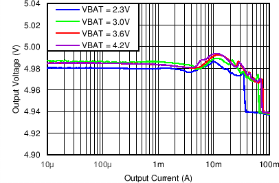
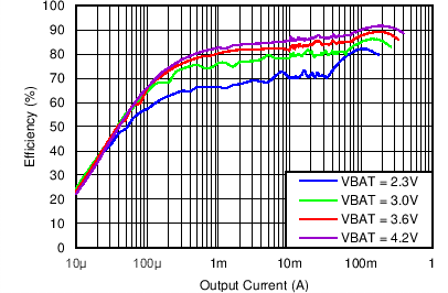
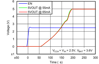
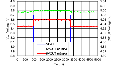
6.12 Typical Characteristics
