ZHCSAD1D October 2012 – June 2017 TPD5S115
PRODUCTION DATA.
- 1 特性
- 2 应用
- 3 说明
- 4 修订历史记录
- 5 Pin Configuration and Functions
-
6 Specifications
- 6.1 Absolute Maximum Ratings
- 6.2 ESD Ratings
- 6.3 Recommended Operating Conditions
- 6.4 Thermal Information
- 6.5 Electrical Characteristics
- 6.6 Electrical Characteristics - I/O Capacitances
- 6.7 Switching Characteristics - VCCA = 1.2 V
- 6.8 Switching Characteristics - VCCA = 1.5 V
- 6.9 Switching Characteristics - VCCA = 1.8 V
- 6.10 Switching Characteristics - VCCA = 2.5 V
- 6.11 Switching Characteristics - VCCA = 3.3 V
- 6.12 Typical Characteristics
- 7 Detailed Description
- 8 Application and Implementation
- 9 Power Supply Recommendations
- 10Layout
- 11器件和文档支持
- 12机械、封装和可订购信息
7 Detailed Description
7.1 Overview
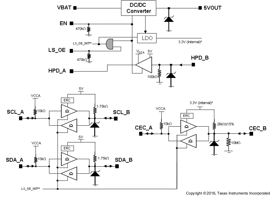
The TPD5S115 is an integrated interface solution that covers HDMI versions' 2.0, 1.4, and 1.3 need for power supply voltage management and control line level translation. On the power supply line, it has a DC-DC converter that takes the internal power supply from 2.3 V to 5.5 V, and outputs a regulated and current-limited, 5‑V voltage to the connector. The drivers support level translation on HPD, ECE, SCL, and SDA lines in both transmission directions. Moreover, the rise-time acceleration feature helps drive the high capacitive load on the cable side. Every channel comes with robust ESD protection with ±14-kV contact and ±16-kV air-gap IEC61000‑4-2 capability.
7.2 Functional Block Diagram

7.3 Feature Description
7.3.1 Rise-Time Accelerators
The HDMI cable side of the DDC lines incorporates rise-time accelerators to support the high capacitive load on the HDMI cable side. The rise-time accelerator boosts the cable-side DDC signal, independent of which side of the bus is releasing the signal.
 Figure 12. Receiving and Transmitting Interaction
7.3.2 Hot Plug Detect
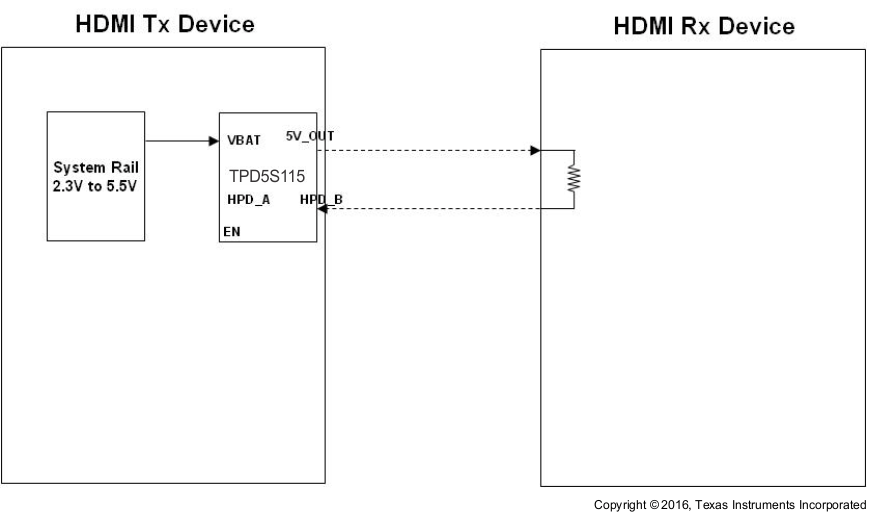
After the TPD5S115’s DC-DC converter and HPD block are enabled through the EN pin, the TPD5S115 is ready for continual HDMI receiver detection. After a HDMI cable connects a receiving and transmitting device together, the 5-V signal from the DC-DC output flows through the receiving device’s internal resistor and into HPD’s input. The HPD buffer’s output then goes high, indicating to the transmitter that a receiving device is connected. To save power, periodic detection can be done by turning on and off the DC-DC converter before a receiving device is connected.
NOTE
Ground offset between the TPD5S115 ground and the ground of devices on port A of the TPD5S115 must be avoided. A CMOS or NMOS open-drain capable of sinking 3 mA of current at 0.4 V has an output resistance of 133 Ω or less (R = E / I). Such a driver shares enough current with the port A output pulldown of the TPD5S115 to be detected as a LOW while the ground offset is zero. If the ground offset is greater than 0 V, then the driver resistance must be less. Because VILC can be as low as 90 mV at cold temperatures and the low end of the current distribution, the maximum ground offset should not exceed 50 mV. Bus repeaters that use an output offset are not interoperable with the port A of the TPD5S115 as their output LOW levels are not recognized by the TPD5S115 as a LOW. If the TPD5S115 is placed in an application where the VIL of port A of the TPD5S115 does not go below its VILC it will pull port B LOW initially when port A input transitions LOW but the port B will return HIGH, so it does not reproduce the port A input on port B. Such applications must be avoided. Port B is interoperable with all I2C-bus slaves, masters, and repeaters.
7.3.3 CEC Level Shift Operation
The CEC level shift function operates in the same manner as the DDC lines except that the CEC line does not need the rise time accelerator function.
7.3.4 Pullup Resistor
The system is designed to work properly with no external pullup resistors on the DDC, CEC, and HPD lines.
7.3.5 Undervoltage Lockout
The undervoltage-lockout circuit prevents the DC-DC converter from malfunctioning at low input voltages and from excessive discharge of the battery. It disables the output stage of the converter once the falling VIN trips the undervoltage-lockout threshold (VBATUV). The undervoltage-lockout threshold for falling VIN is typically 2 V. The device starts operation once the rising VIN trips the under-voltage-lockout threshold again at 2.1 V (typical).
7.3.6 Soft Start
The DC-DC converter has an internal soft-start circuit that controls the ramp-up of the output voltage. The output voltage reaches its nominal value within 250 µs (typical) after EN has been pulled high. The output voltage ramps up from 5% to its nominal value within 300 µs (typical). This limits the in-rush current in the converter during start-up and prevents possible input voltage drops when a battery or high impedance power source is used. During soft start, the switch current limit is reduced to 300 mA until the output voltage reaches VIN. Once the output voltage trips this threshold, the device operates with its nominal current limit.
7.4 Device Functional Modes
7.4.1 Power-Save Mode
The TPD5S115 integrates a power-save mode to improve efficiency at light loads. In power-save mode, the converter only operates when the output voltage trips below a set threshold voltage. It ramps up the output voltage with several pulses and goes into power-save mode once the output voltage exceeds the set threshold voltage. The PFM mode is ended and PWM mode begins in case the output current can no longer be supported in PFM mode.
7.4.2 Enable
The DC-DC converter is enabled when the EN is set to high. At first, the internal reference is activated and the internal analog circuits are settled. Afterwards, the soft start is activated and the output voltage is ramped up. The output voltage reaches its nominal value in 250 µs (typical) after the device has been enabled. The EN input can be used to control power sequencing in a system with various DC-DC converters. The EN pin can be connected to the output of another converter to drive the EN pin high and create a sequencing of supply rails. When EN = GND, the converter enters shutdown mode.